Facebook
 Google
 GitHub
 Linkedin
Optimizing Control of Both the Synchronous Rectifier and Primary MOSFET in Flyback Power Supplies Improves Efficiency and Reliability
This article offers methods overcoming the limitations of Schottky diode rectifier designs without the complexity of traditional synchronous rectifier ways.
Designers of flyback power supplies have generally used Schottky diode rectification in the output stage due to its simplicity and low cost. Diode-rectifier designs have proven adequate in meeting the efficiency demands of yesteryear, particularly for low current (0.5-1 A) outputs.
New market requirement
However, as regulators take aim at the operating efficiency of small power supplies used in stand-alone charger/adapters and as bias supplies for high power applications, the impressive performance of synchronous rectification becomes very attractive. Smartphones with larger screens and much higher performance provide a great example of a device that requires an increase in power and a tightening of efficiency rules, while enjoying a phenomenal rise in popularity. Smartphone battery size has increased by more than 300 % from a typical capacity of 700-900 mAhr just a few years ago to around 3000 mAhr today. For phablets and tablets, it is even higher, ranging from 6000 to 10,000 mAhr. This is driving an increase in the power supply rated current - up to 400% in some cases - from 5 watts USB (5 V, 1 A) for traditional adapters to 10-20 watts (5 V, 2-4 A) for rapid charging devices.
In addition to the higher power and current, new stringent efficiency regulations such as mandatory DOE-6 (Department of Energy - Level 6) in USA and CoC V5 Tier 2 regulation in Europe have now created a pressing need for much higher efficiency.
This combination of higher power requirement, higher performance and compact size with low external touch-temperature - while still meeting the new efficiency regulations - has challenged Schottky rectifier implementations in both performance and cost.
Schottky diode vs. SR (Synchronous Rectifier)
Schottky diodes typically have a forward voltage drop of 0.4 to 0.5 V which means that in a standard 5 V output just the Schottky diode alone can result in a power loss of up to 10 %.
Synchronous Rectification (SR) can be used to boost the efficiency and reduce the heat by eliminating the lossy Schottky diodes and replacing them with an actively controlled SR MOSFET. This is made possible by the very low resistance, RDS(on) of SR MOSFETs when conducting – down to below 10 mΩ. So the forward drop in an SR MOSFET can be just 20-40 mV for a 2-4 A output current. In high current applications, this represents a dramatic reduction in power loss from 10 % for a Schottky diode to less than 1 % for an SR FET – a 10-fold improvement. Therefore, an SR technique together with secondary side regulation control is suited to enable improvements in efficiency and thermal performance. However, the complexity and cost of traditional SR has prevented its wider adoption, restricting it to complex and higher power designs.
Limitations of traditional Synchronous Rectifier (SR) alternatives
The complexity of traditional SR architecture stems from the fact that the timing control in a traditional SR FET architecture is very difficult. When comparing non-synchronous and synchronous rectifiers, it is important to understand that the synchronous rectification MOSFET doesn’t simply replace the traditional Schottky diode: complex control circuitry is also required to sense and then drive the MOSFET at the correct instant to allow current to flow only in the correct direction.
Any time that the primary side FET turns on before the secondary side FET has turned off, it will cause simultaneous conduction in both the secondary and primary circuit. This effective short-circuit across the primary transformer winding results in the dreaded “shoot-through” that will destroy the primary FET. On the other hand, once the primary FET turns off if there is a delay in turning on the secondary SR FET the result is a reduction in efficiency. So designers are faced with a difficult dilemma and a significant increase in design complexity is required to overcome these design challenges.
Traditional SR solutions deploy a separate secondary-side controller to drive the SR FET. This adds cost and complexity to the circuit, restricting its uptake due to the extra cost burden. Also, with two separate controllers these designs include a delay period, called “dead-time”, providing margin and preventing switching overlap of the primary and secondary MOSFETs (shoot-through) that can result in highly destructive cross-conduction currents. The synchronous rectification MOSFET contains an integral, parasitic body diode that operates during this dead time. Unfortunately, this body diode is also lossy and slow to turn off, so it too can contribute a 1 % to 2 % drop in efficiency. To overcome this loss in efficiency a small Schottky diode, which conducts only during the dead time, can be placed in parallel with the synchronous rectification MOSFET, ensuring that the body diode never conducts. The Schottky diode used in this way is smaller and cheaper than the part required for a diode rectification design because the average diode current is low, however, an efficiency loss of >0.5 % can still be expected.
So although traditional synchronous rectification (SR) has some obvious advantages, it can be very difficult to implement because the timing of the MOSFETs turn-off signal is so critical. For optimum performance, it is necessary to know exactly when the primary switch is on and off. Although the state of the MOSFET can be inferred from the secondary winding, this approach does not provide the accuracy required. If a conservative prediction is made efficiency suffers; if an overly-aggressive prediction is made, shoot-through can occur. This is challenging during normal operation but it becomes increasingly difficult to guarantee shoot-through doesn’t occur under transient conditions such as output short- circuit, start-up, AC line drop outs and load steps.
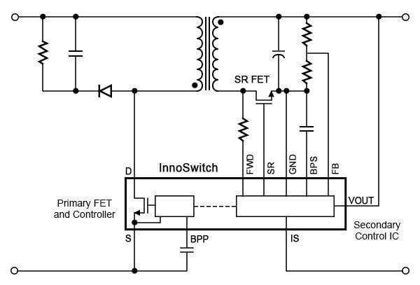
Figure 1: InnoSwitch – Single IC with integrated SR and feedback
An Innovative new approach
But this is about to change with Power Integrations’ new InnoSwitch™ family of ICs. For the first time, users have a shoot-through-proof design with the simplicity of a single integrated IC (Figure 1) that completely controls both the primary and secondary FET rather than two separate primary and secondary controller ICs with optocoupled SSR (secondary side regulation). This single IC also incorporates a very high bandwidth communication link between the primary and secondary controllers - called FluxlinkTM. This high-speed digital communication link is incorporated in the device package through a magnetic coupling but without any magnetic cores. The material used for the manufacture of the IC package remains the same. The secondary controller acts as the master which initiates the switching process for both the secondary and primary MOSFETs, so no prediction or inference as to the state of the two MOSFETs is required. It is shoot-through-proof because the two MOSFETs are controlled deterministically and never turned on simultaneously. Using this innovative and near-instantaneous communication afforded by FluxLink technology provides the secondary controller precise control of both primary MOSFET and the secondary SR MOSFET. The system achieves almost optimum turn-on and turn-off times across the entire load range, whether the power supply is operating in discontinuous mode, continuous mode, and even under fault conditions. Therefore, the power supply is intrinsically safe and it is always working at maximum efficiency.
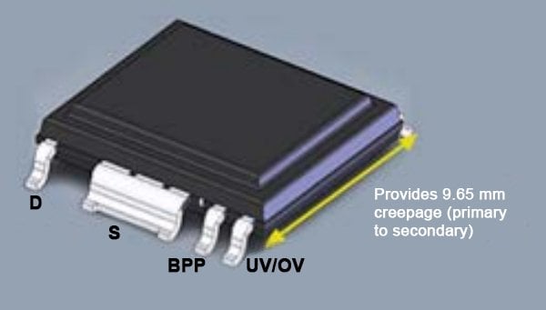
Figure 2: InnoSwitch ICs enable designs to meet all global safety standards
InnoSwitch ICs also maintain full internal galvanic isolation and are safety approved to UL1577, TÜV60950. They also meet the CQC China 5,000 meter altitude requirement for creepage (see Figure 2). An external pin-to-pin creepage gap of over 9.65 mm is achieved using a custom surface-mount package that has been specially designed for this IC family (Figure 2).
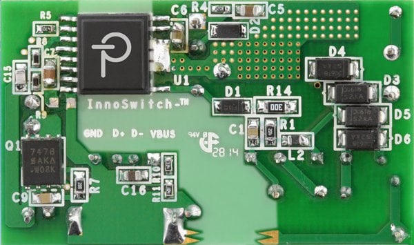
Figure 3: An InnoSwitch IC is placed across an isolation area
Being a recognized safety component the InnoSwitch ICs can be placed in the primary-to-secondary isolation barrier area on the PCB, so effectively the ICs take up no useable space at all (Figure 3). Also, the design allows for direct and simple resistor divider sensing of the power supply output voltage with excellent load transient performance and keeps the no-load power consumption below 10 mW. Direct sensing is significant as it reduces the physical volume of the output capacitors required, critical to fitting designs in ever-shrinking enclosure sizes. The power supply output current measurement in an InnoSwitch IC is fully integrated inside the package, eliminating external current sense circuitry altogether. This results in higher power density, reliability and improved manufacturability.
| Summary of InnoSwitch Benefits |
| High efficiency: Meets all global safety standards |
| High performance: Fast transient response with secondary side control |
| High reliability: Shoot-through-proof design |
| Very low No-load: Less than 10mW |
| Low component count: Just 30 components for a 5V, 2A adapter design |
| Improved manufacturability: Simpler and variation-tolerant transformer design |
| Elimination of SR FET parallel diode: Lower cost |
| No extra components required for high output voltages: Forward pin supports 12V output |
Table 1: InnoSwitch IC benefits
Now synchronous rectification can be used safely and reliably in higher power chargers, even those with adaptive voltage outputs such as Qualcomm’s Quickcharge™ 2.0 and MediaTek™ PE+. The ability to deliver high currents at high efficiency also makes InnoSwitch an excellent fit for the newly announced USB-PD standard that requires support for 3 A and 5 A output load currents.
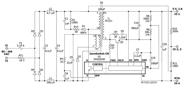
Figure 4: 5 V, 2 A adapter – just 30 components, see sidebar for full details
In summary, InnoSwitch ICs combine the benefit of an advanced Synchronous Rectification (SR) technique with secondary side control and communication link into a single IC to meet new market requirements for higher power, performance, density, reliability and efficiency (see Table 1). These benefits and, indeed, the use of InnoSwitch ICs are not limited to cell phone adapters. This new powerful architecture can also be used in any application that demands greater efficiency with higher secondary currents (>1.5 A).
About the Author
Silvestro Fimiani works as the Senior Product Marketing Manager at Power Integrations. He is responsible for the industrial product, motor control and appliance. He is particularly skilled in the field of semiconductors, product development and marketing. He earned his Bachelor's Degree in Physics at the University of Naples 'Federico II'. He also received his certification in machine learning and practical time series analysis from Coursera.