Facebook
 Google
 GitHub
 Linkedin
Optimized Sigma-Delta Modulated Current Measurement for Motor Control – Part 2
In Part 2 of the series, a sinc filter structure optimized for synchronization is proposed. The filter improves measurement performance in applications that require tight timing control of the feedback chain. Part 2 then moves on to discuss the implementation of sinc filters using HDL code and how to optimize the filters for FPGA implementation. Finally, measurement performed on an FPGA-based 3-phase servo drive are presented.
Sinc Filters Optimized for Synchronization
As discussed in Part 1, an alias-free sigma-delta measurement is possible through the correct alignment of the sinc filter impulse response to PWM. While the method is straightforward, it is difficult—and in many cases impossible—to find a system configuration that gives the desired result. To illustrate this, assume the sinc filter and the PWM block shares a common system clock source that runs at fsys. The modulator clock, fmclk, is then determined by Equation 1.1
$$f_{mclk}=\frac{f_{sys}}{D_{mclk}}$$
Equation 1.
Where Dmclk is the clock divider for the modulator clock. Similarly,
$$f_{pwm}=\frac{f_{sys}}{D_{pwm}}$$
Equation 2.
Where DPWM is the clock divider determining the PWM frequency. Finally, the decimation rate (data rate) from the sinc filter is given
$$f_{dec}=\frac{f_{mclk}}{D_{dec}}=\frac{f_{sys}}{D_{mclk}\times D_{dec}}$$
Equation 3.
Where Ddec is the clock divider for the decimated clock. To avoid drift between the impulse response and the PWM cycle, there must
$$\frac{f_{dec}}{f_{pwn}} = N$$
Equation 4.
Where N is an integer. By combining Equation 2, Equation 3, and
$$\frac{D_{pwm}}{D_{mclk}\times D_{dec}} = N$$
Equation 5.
Clearly, only a limited selection of clock scalers, Dx, satisfy Equation 5. Furthermore, most often there are tight restrictions on how the clock scalers can be selected. For example, a system may be required to run at a certain PWM frequency (for example, 10 kHz) or use a certain modulator clock (for example, 20 MHz). Another complication is the limited number of options when it comes to selecting the modulator clock. For example, if fsys is 100 MHz, the only reasonable choices for Dmclk falls in a limited range of integers of 5 to 10 (20 MHz down to 10 MHz).
Given all these restrictions, it is very difficult—if not impossible—to find clock scales that give the desired alignment between impulse response and PWM. What typically happens is the user is forced to select clock scalers that satisfy Equation 5 rather than selecting clock scales that result in the desired PWM frequency, modulator clock, and signal-to-noise ratio (SNR). Also, if one of the frequencies changes over time, it becomes impossible to find a valid configuration. This is quite common in multiaxis systems where a single motion controller synchronizes multiple motor controllers in a network.
While the alignment scheme gives excellent measurement performance, it can prove to be impractical. In the following section, a new type of sinc filter is presented. The filter offers optimum measurement performance and at the same time allows the user to select all clock dividers independently.
Flushing Sinc Filter
A traditional third-order sinc filter is shown in Figure 1. The filter generates the modulator clock to the ADC by scaling the system clock and, in return, the ADC generates a 1-bit data stream to the filter. The filter function itself consists of three cascaded integrators, 1/(1 – z–1), clocked at the same rate as the modulator and three cascaded differentiators, 1 – z–1, clocked at the decimated clock.
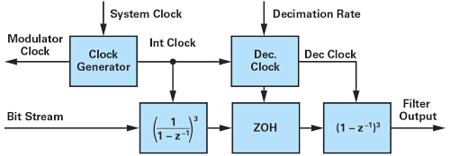
Figure 1. Traditional third-order sinc filter. Image used courtesy of Bodo’s Power Systems
The sinc filter and ADC are operated by continuously applying a clock to both. As a result, the filter outputs data continuously at a fixed rate determined by the decimated clock. The data rate from the filter is typically higher than the update rate of the motor control algorithm, so a number of the filter outputs are rejected. Only when the impulse response is centered around the ideal measurement is the output captured and used as feedback.
With space vector modulation, the phase current only assumes its average value two times per PWM period. Following this, there are only two possible alias free sinc data output per PWM cycle, so there is no need to let the filter run continuously. It is actually sufficient to only enable the measurement when the feedback is needed and then disable the measurement at all other times. In other words, the measurement operates in an on-off mode, not unlike a conventional ADC.
A problem with the on-off mode of operation is that the modulator and filter clocks are derived from the same system clock. That means both the filter and the ADC operate in an on-off mode, which is not recommended because it will result in reduced performance. The reason is that the modulator in the ADC is a higher order system with a certain settling time and damping. So, when first applying a clock to the ADC, the modulator needs to settle before the output bit-stream can be trusted. To solve these problems, a new filter structure is proposed (see Figure 2).
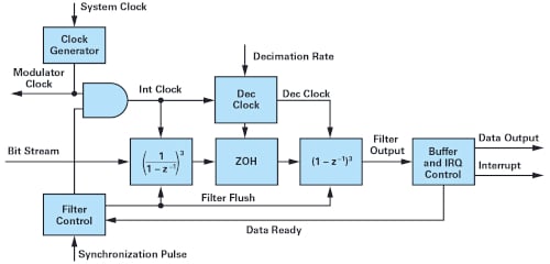
Figure 2. Sinc filter designed for on-off operation and flush of all states. Image used courtesy of Bodo’s Power Systems
As the standard sinc filter, the core consists of three cascaded integrators and three cascaded differentiators. However, the filter has several features that allow for new operating modes. Firstly, the filter has a new clock generator function that separates the modulator clock from the integrator clock. That makes it possible to continuously clock the ADC, but only enables the integrator clock when obtaining a measurement. Secondly, the filter has a new filter control function. With reference to a synchronization pulse, the control block handles all timing and triggering needed to operate the filter. The primary function of the filter controller is flushing the filter, which involves initializing all filter states, and timers filter ahead of starting a new measurement, as well as enable/disable the integrator clock at the right instances. Finally, the filter has a new buffer and interrupt control unit, which sorts through the output data and captures the correct measurement. The buffer and interrupt unit also notifies the motor control application by interrupting when a new measurement is ready to be consumed. The timing diagram in Figure 3 shows how the filter operates.
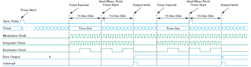
Figure 3. Timing diagram of sinc filter operating in an on-off mode. Image used courtesy of Bodo’s Power Systems
To start a measurement a synchronization pulse (sync pulse) is applied to the filter controller. Typically, this pulse indicates the start of a new PWM cycle. The sync pulse starts a timer, which is configured to expire exactly 1.5 decimation cycles before the desired measurement point. At this point, the integrator clock and decimated clock are enabled and the filtering process begins. After 3 decimation cycles (the settling time of a third-order sinc filter), the buffer and interrupt controller captures the data output and asserts the interrupt. In Figure 3, notice how the measurement is centered around the sync pulse. The sequence repeats itself at the next sync pulse, but the modulator clock remains on once the filter has been started.
The proposed sinc filter solves the problem of synchronization of a conventional sinc filter. The filter and its operating mode do not make any assumptions about the PWM frequency, the modulator clock, or the decimation rate. It works equally well with all system configurations and even if the PWM frequency varies over time. Since the filter is effectively reset for every measurement, it is also insensitive to drift between the clocks.
HDL Implementation of Sinc Filters
The authors have found that several of the publicly available sinc filter HDL examples have shortcomings that negatively affects filter performance or leads to unexpected behavior. This section will discuss some of the implementation issues and how to design HDL code for optimum performance on an FPGA.
Integrators
In its purest form a sinc3 filter consists of three cascaded integrators and three cascaded differentiators, see Figure 1. First, consider a pure integrator in the z-domain2:
$$\frac{y(z)}{u(z)} = \frac{1}{1-z{^{-1}}}$$
Equation 6.
Where u is the input and y is the output. The integrator has the difference equation:
$$y[n]=u[n]+y[n-1]$$
Equation 7.
This first order equation is equivalent to an accumulator, which lends itself very well to implementation in clocked logic such as an FPGA. A common implementation approach is a D-type flip-flop accumulator as shown in Figure 4.
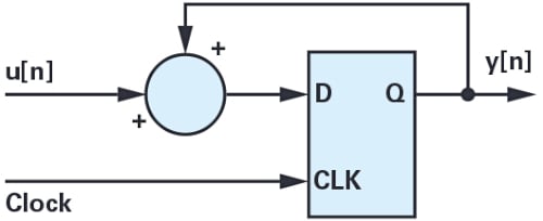
Figure 4. Implementation of an accumulator with a D-type flip-flop. Image used courtesy of Bodo’s Power Systems
This circuit can be implemented on an FPGA with only few logic gates. Now, when cascading three pure integrators, the transfer function in the z-domain is defined by Equation 8.
$$\frac{y(z)}{u(z)} = \bigg(\frac{1}{1-z{^{-1}}}\bigg){^{3}}=\frac{1}{1-3z{^{-1}}\,+\,3z{^{-2}}-z{^{-3}}}$$
Equation 8.
The difference equation for the three cascaded integrators is shown in Equation 9:
$$y[n]=u[n]+3y[n-1]-3y[n-2]+y[n-3]$$
Equation 9.
Notice how the input at sample n affects the output at sample n.
If the three integrators are implemented with the D-type flip-flip accumulator in Figure 4, the result is as shown in Figure 5.
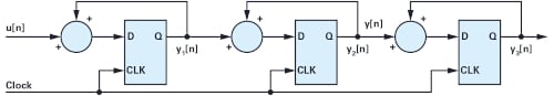
Figure 5. Three cascaded accumulators implemented with D-type flipflops. Image used courtesy of Bodo’s Power Systems
Since this is a clocked circuit, it will take several clocks for a change of the input to affect the output. This becomes even clearer when examining the difference equations for the cascade accumulators (see Equation 10).
$${y_{1}}[n]=u[n]+{y_{1}}[n-1]$$
$${y_{2}}[n]={y_{1}}[n-1]+{y_{2}}[n-1]=u[n-1]={y_{1}}[n-2]+{y_{2}}[n-1]$$
$${y_{3}}[n]={y_{2}}[n-1]+{y_{3}}[n-1]=u[n-2]+{y_{1}}[n-3]+{y_{2}}[n-2]+{y_{3}}[n-1]$$
Equation 10.
This difference equation is quite unlike the one for the pure integrators (see Equation 9). With the accumulators, it takes two clocks before an input affects the output, whereas with pure integrators, the input affects the out immediately. To illustrate this, Figure 6 shows the step response of Equation 9 and Equation 10, respectively, when a unit step is applied at sample number 5. As suspected, the accumulators are delayed by two samples compared to the integrators.
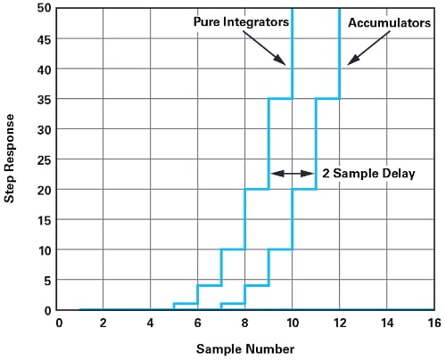
Figure 6. Step response of three cascaded integrators and three cascaded accumulators. Image used courtesy of Bodo’s Power Systems
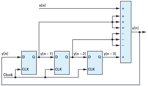
Figure 7. Implementation of three cascaded integrators. Image used courtesy of Bodo’s Power System
In most publicly available sinc filter examples, it is recommended to implement the integrators with D-type flip-flop accumulators. The main argument for this is low gate count, but the lightweight implementation comes at a cost. Compared to the filter’s group delay, an additional delay of two modulator clocks may seem insignificant, but the delay impacts the filter’s ability to attenuate higher frequencies, and as a result, the accumulator implementation gives fewer effective numbers of bits than a pure integrator would. Furthermore, the proposed flushing sinc filter requires an ideal transfer function in order to work correctly. For those reasons, no sinc filter implementation should rely on accumulators to implement the integrator stage.
To get the ideal sinc3 response, a direct implementation of the difference from Equation 9 is proposed. The result is shown in Figure 7. Note how the block diagram consists of two parts: a clocked logic part (the flip-flops) and a combinatorial part (the summations). This realization requires more gates, but it has the desired filter performance and delay.
Differentiators
Similar to the integrators, many of the publicly available sinc filter examples implement the differentiator stage incorrectly, which results in reduced filter performances and unexpected delay. This section discusses the differentiator stage and makes recommendations on how to implement an FPGA for optimum performance. First, consider a pure differentiator in the z-domain in Equation 11 and the corresponding difference in Equation 12.2
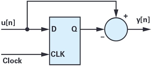
Figure 8. Differentiator implemented with D-type flip-flop. Image used courtesy of Bodo’s Power System
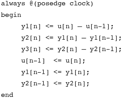
Figure 9. Three differentiators implemented as clocked logic. Image used courtesy of Bodo’s Power System
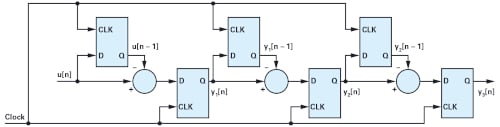
Figure 10. Differentiators implemented with clocked assignments. Image used courtesy of Bodo’s Power System
$$\frac{y(z)}{u(z)}=1-{z^{-1}}$$
Equation 11.
$$y[n]=u[n]-u[n-1]$$
Equation 12.
To realize a differentiator on an FPGA a D-type flip-flop is most commonly used, see Figure 8.
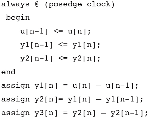
Figure 11. Three differentiators implemented as a mix of clocked logic and combinatorial logic. Image used courtesy of Bodo’s Power System
A common way to implement the three D-type flip-flop differentiators is illustrated with the following HDL code snippet. Here, pseudo-Verilog is used, but the principles applies to other languages, too.
As with any clocked assignment, all the right-hand side statements are evaluated first and assigned to the left-hand side.3 Everything is clocked and all assignments are updated in parallel. This is a problem because the output terms (yx[n]) relies on the delayed terms (u[n-1] and yx[n-1]) being updated first. As a result, the previous Verilog snippet implements to logic, as shown in Figure 10.
Due to the clocked assignments, the delay of the differentiators is six clocks rather than the expected three clocks. Since the differentiators are clocked with the decimated clock, this effectively doubles the filter’s group delay and settling time. However, it also affects the filter’s attenuation and the frequency response is not that of an ideal third-order sinc. The implementation in Figure 10 is often seen in published sinc filter examples, but it is highly recommended to choose an approach that mimics an ideal differentiator stage.
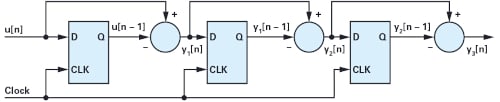
Figure 12. Implementation of three cascaded differentiators using a mix of clocked logic and combinatorial logic. Image used courtesy of Bodo’s Power System
The previous Verilog code snippet can be separated into two parts: a combinatorial part that calculates the current outputs and a clocked logic part that updates delayed states. This separation makes it possible to move the combinatorial part outside the always clocked block as shown in the code snippet shown in Figure 11.
With the combinatorial assignments, there is no additional delay associated with the calculation of yx and the total delay is brought down from 6 clocks to the ideal 3 clocks. The block diagram for the recommended implementation of the differentiators is shown in Figure 12.
By combining the proposed implementation of the cascaded integrators and differentiators, the sinc filter gets ideal characteristics in terms of attenuation and delay. All sigma-delta-based measurements will benefit from the optimized filter implementation, but especially the flushing sinc that relies on knowing the exact filter delay.
Measurements
The proposed sigma-delta measurement system has been implemented and tested together with a servo motor controller based on a Xilinx® Zynq®-7020 SoC.4 The system consists of a 60 V, 3-phase permanent magnet servo motor (Kinco SMH40S 5) and a 3-phase switching voltage source inverter. The SoC runs a field-oriented motor control algorithm, as well as software for capturing measurement data in real-time.
For phase current measurement, the system has two isolated sigma-delta ADCs (ADuM7701) followed by two third-order sinc filters. The sinc filters are implemented using the design recommendation discussed in this article, including the flushing sinc mode of operation. For comparison, measurement results for both the traditional, continuously operating filter and the flushing filter will be presented.
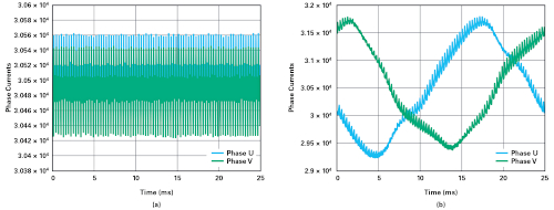
Figure 13. Continuous operating mode with the sinc filter impulse response unaligned to PWM. Image used courtesy of Bodo’s Power System
While the control system has closed loop field-oriented control, all measurements are performed with the open-loop control. A closed current loop is sensitive to measurement noise and the noise will couple through the current loop. By operating in open-loop, any effects from the current controllers are eliminated, which makes it possible to compare results directly.
Except for mode configuration and alignment to PWM, the measurements were done with the identical configurations including the decimation rate, which was set to 125. Any difference in the measurement results can therefore be contributed to the effect of aligning the sinc3 impulse response correctly to PWM or not. The control algorithm is executed at 10 kHz and the modulator clock is 12.5 MHz.
Unaligned Impulse Response with Continuous Sinc Filter Operation
In the first example (see Figure 13a), the impulse response is uncorrelated to the PWM waveform. Figure 13b shows two phase current measurements when the motor is stopped but the power inverter is switching with a duty cycle of 50% on all phases. In this operating mode, the measurement shows the noise level of the measurement. Figure 13b shows the phase currents when the motor is running open-loop at 600 rpm. The motor has four pole pairs, so the electrical period is 25 ms. Both plots show significant noise that would severely affect the performance of any closed-loop current controller. The noise level is unrelated to the magnitude of the fundamental phase current, so the noise is relatively worse at light load. The noise in this example is due to an unaligned sinc filter impulse response and it would have little or no increase to the decimation rate (attenuation) of the sinc filter.
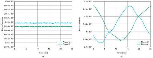
Figure 14. Continuous operating mode with sinc filter impulse response aligned to PWM. Image used courtesy of Bodo’s Power System
Aligned Impulse Response with Continuous Sinc Filter Operation
Figure 14 shows measurement results when there is an integer number of decimation cycles per PWM period and the impulse response is aligned with the ideal measurement point. The results in Figure 14 are directly comparable with the results in Figure 13.
When comparing Figure 13 and Figure 14, the filters are using the same decimation rate, but the noise level has been reduced significantly. The examples illustrate how important system configuration and synchronization are to fully utilize the performance of a sigma-delta-based signal chain.
Flushing Sinc Filter
While the results for the continuously operating sinc filter in Figure 14 were satisfactory, the filter still has difficulty in finding a configuration that enables synchronization. While it is possible to synchronize a continuously operating sinc filter to PWM, it is often not practical. That problem is solved with the flushing sinc filter.
Figure 15 shows measurement results for a flushing sinc filter. The filter is configured to only run for 3 decimation cycles around the ideal measurement point. Performance is, as expected, similar to the continuously operating filter in Figure 14.
For comparison, the flushing filter uses the exact same configuration as the continuously operating filter. The difference is that the continuously operating filter must use this configuration or performance will deteriorate, as illustrated by the results in Figure 13. The flushing filter, on the other hand, will maintain its optimal performance with any possible system configuration.
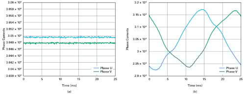
Figure 15. Flushing sinc filter with sinc filter impulse response aligned to PWM. Image used courtesy of Bodo’s Power System
The magnitude of the noise with the unaligned, continuously operating sinc filter (Figure 13a) is approximately 120 counts out of a 16-bit signal. That corresponds to a loss of approximately the lower 7 bits due to noise. The noise level of the flushing sinc filter (Figure 15a) is approximately 5 counts out of a 16-bit signal, corresponding to losing less than 3 bits due to noise.
Summary
Sigma-delta-based phase current measurement is widely used in motor drives, but getting optimum performance requires correct configuration of the whole system. This article discussed the sources that can lead to poor performance and how to correctly set up a system.
Configuring a system for optimum current feedback performance can be challenging and, in some cases, impossible. To solve this, a new type of sinc filter was proposed. The filter operates in an onoff mode and guarantees optimum performance with any system configuration.
Implementing a sinc filter on an FPGA requires development of HDL code. The article discussed several implementation techniques that lowers delay in the filter and increases attenuation.
This article originally appeared in Bodo’s Power Systems magazine.