Facebook
 Google
 GitHub
 Linkedin
Optimized Sigma-Delta Modulated Current Measurement for Motor Control – Part 1
This article is Part 1 in a series of two. It discusses demodulation of sigma-delta coded data using sinc filters in a motor control application. It then takes a close look at different approaches for since filter and control algorithm synchronization.
Isolated sigma-delta (∑-Δ)-based analog-to-digital converters (ADCs) have become the preferred method for phase current measurement in high performance motor and servo drives. The converters have deservedly earned a reputation for robust galvanic isolation and excellent measurement performance. With every new generation of ADCs, the performance is increased even further, but to fully utilize the potential of the latest ADCs, the rest of the motor drive needs to be designed accordingly.
Introduction Motor drive manufacturers continue to improve the performance and robustness of their products. Some of the improvements have been realized through more advanced control algorithms and higher computational power. Other improvements have been accomplished by minimizing nonideal effects in the feedback circuits such as latency, skewing, and temperature drift.1
When it comes to feedback for the motor control algorithm, the most critical part is phase current measurement. As control performance increases, the system becomes more and more sensitive to nonideal effects such as timing accuracy, offset/gain errors, and synchronization of multiple feedback channels. Over the years, semiconductor companies have focused on reducing these nonideal effects in the feedback signal chain, and that trend is likely to continue. The ADuM7701 is one example of the latest generation of isolated sigma-delta ADCs optimized for phase current measurement. While the performance of the ADC is important, there is a high risk of introducing nonideal effects in the rest of the feedback path as well. This article goes beyond the ADC and primarily discusses the remaining part of feedback path. While the main focus is on motor control applications, this article applies to any system that requires tight synchronization of sigma-delta ADCs.
The typical signal chain, when using a sigma-delta ADC, is shown in Figure 1.
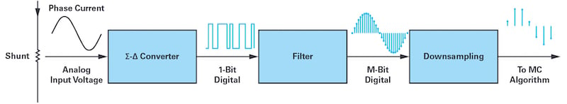
Figure 1. A sigma-delta signal chain for phase current measurement. Image used courtesy of Bodo's Power Systems.
An analog input voltage is created by letting the phase current pass through a resistive shunt. The sigma-delta ADC converts the analog signal into a 1-bit data stream and provides galvanic isolation so everything that follows the ADC is isolated from the motor phase potential. Following the converter is demodulation in the form of a filter. The filter converts the 1-bit signal into a multibit signal (M-bit) and brings the data update rate down through the process of decimation. While the decimation in the filter lowers the data rate, it is typically still too high to match the update rate of the control algorithm. To solve this problem, a final downsampling stage is added.
Sinc Filter Synchronization
Sigma-delta ADCs and sinc filters are criticized for being difficult to control in the time domain and for their lack of a defined sampling instant.2 When compared to a conventional ADC with a dedicated sample-and-hold circuit, there is some reason for concern. However, there are ways to work around this. As will be shown in this section, it is crucial to synchronize the sinc filter to the rest of the system and to sample the phase current at the right instant. If this is not done correctly, the resulting measurement will suffer from significant distortion.
The output from a sinc filter is not a representation of what the input to the sigma-delta ADC is at that instant. Rather, the output is a weighted average of what the input was during a windowed period in the past. This behavior is due to the filter’s impulse response. Figure 2a shows the impulse response of a sinc3 with a decimation rate of 5. The figure shows how the filter output is a weighted sum of the input sequence that gives more weight to samples at the center and less weight to samples at the beginning/end.
Before proceeding, a few basic definitions are needed. The sigmadelta ADC clock, also called the modulator clock, is referred to as fmod. The decimation rate (DR) determines the decimation frequency (fdec) and is linked to fmod, as shown in Equation 1:
\[DR = \frac{f_{mod}}{f_{dec}}\]
Equation 1
The right side of Figure 2 shows the effect the impulse response has on the filter’s step response.
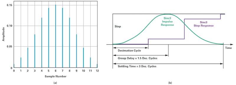
Figure 2. (a) Sinc filter impulse response for a filter with a decimation rate of 5. (b) Sinc filter step response and relation to impulse response. Image used courtesy of Bodo's Power Systems.
As the step is applied, the filter output is unaffected, and it takes three full decimation cycles before the filter reaches steady state. Based on this, some important properties of a sinc3 filter can be stated:
- The group delay is 1.5 decimation cycles long
- The settling time is 3 decimation cycles long
These properties are important when it comes to synchronizing the filter to the control system and they will be utilized throughout the article.
Before discussing sinc filter synchronization, the characteristics of the input signal must be defined. This in turn will define what the filter must be synchronized to.
Figure 3 shows a simulated phase current of a 3-phase permanent magnet motor driven by a voltage source inverter. The modulation scheme is space vector PWM3 and the switching frequency is 10 kHz. The motor is loaded to 5 A peak phase current and the rotational speed is 3000 rpm. This setup, along with 3 pole pairs, results in an electrical fundamental period of 6.67 ms.
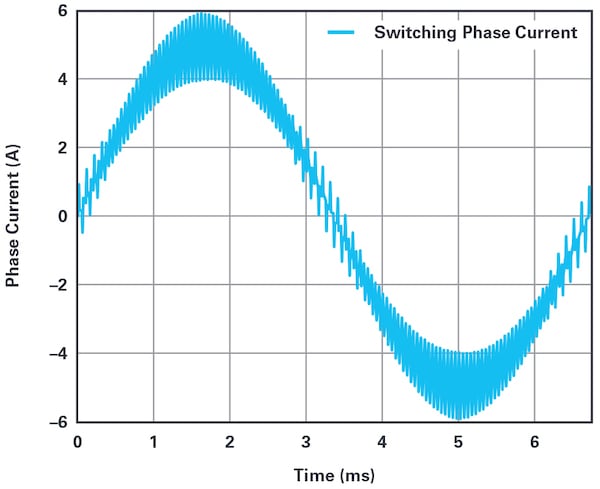
Figure 3. Motor phase current with space vector pulse-width modulation. Image used courtesy of Bodo's Power Systems.
The phase current can be seen as two components: an average and a switching component. For control purposes, only the average component of the current is of interest, so the switching component must be fully removed. The most common way to extract the average component is to sample the signal synchronized to the PWM waveform applied to the motor terminals. This is illustrated in Figure 4.
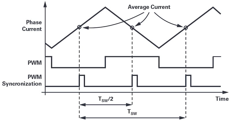
Figure 4. Measuring phase current at the beginning and center points of a PWM period attenuates the current ripple. Image used courtesy of Bodo's Power Systems.
The top signal shows the switching waveform of a phase current, the middle signal shows a high-side PWM signal for the corresponding inverter phase leg, and the lower signal shows the synchronizing signal from the PWM timer. The PWM synchronization signal is asserted at the beginning and the center of a PWM cycle. For simplicity, it is assumed that all three phases run with a duty cycle of 50%, which means there is only one rising slope and one falling slope of the current. At the rising edge of the PWM synchronization signal, the current assumes its average value, so if the currents are sampled at exactly that moment, the switching component will be fully suppressed. Effectively, the sample-and-hold circuit is equivalent to a filter with infinite attenuation at the switching frequency.
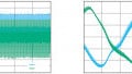
Figure 5 shows the result of what happens when this kind of sampling is applied to the waveform appearing in Figure 3. The right side shows a close-up of the actual phase current and the sampled current. Note how the sample-and-hold process completely removes the ripple.
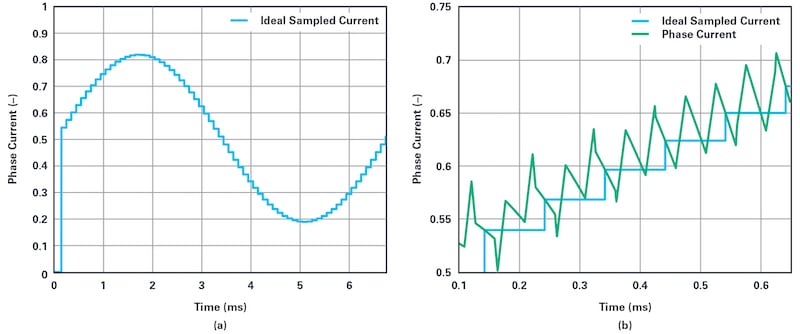
Figure 5. Ideal sampling of phase current: (a) a fundamental period of ideally sampled phase current, (b) a close-up look at phase current and sampled phase current. Image used courtesy of Bodo's Power Systems.
Per-unit representation of the sampled current is used where 0 A is mapped to 0.5 and the full scale is 8 A. This scaling is chosen for easier comparison to the sigma-delta measurements that follow. The result shown in Figure 5 is the ideal scenario, with only the fundamental component left after sampling. As such, these data can be considered the benchmark to which the sigma-delta measurements will be compared.
Sigma-Delta Measurement and Aliasing
With the ideal sample-and-hold ADC, it is possible to extract the fundamental component because of tight control of the sampling instant. However, sigma-delta conversion is a continuous sampling process and the ripple component will inevitably be part of the measurement.
With sigma-delta conversion there is a close link between the decimation rate and signal-to-noise ratio (SNR). The higher the decimation rate, the more effective number of bits (ENOB) of the output. The downside is, as the decimation rate increases, the group delay also increases so the designer must compromise between signal resolution and delay in the feedback chain. As a general rule, the delay must be kept small compared to the control cycle period. For motor control, typical decimation rates fall in the range of 128 to 256, which provides a good compromise between SNR and group delay.
For data sheet specifications, a decimation rate of 256 is commonly used. For example, ADuM7701 has an ENOB of 14 bits, at a decimation rate of 256. With such a high ENOB number, a very clean measurement is to be expected. To verify this, suppose the phase current shown in Figure 3 is measured with a sigma-delta ADC clocked at 20 MHz and that the data stream is demodulated by a sinc3 using a decimation rate of 256. The result is shown in Figure 6a.
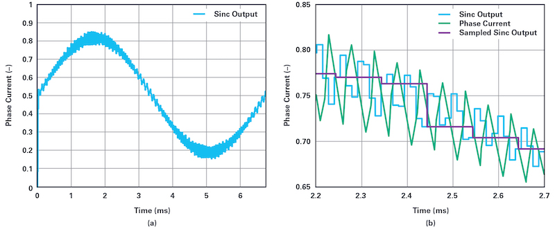
Figure 6. (a) The output from the sinc filter. (b) A close-up look at the actual phase current and decimated output from the sinc filter. Image used courtesy of Bodo's Power Systems.
The fundamental component of the phase current is obvious, but the measured signal is very noisy when compared to the ideal sampling shown in Figure 5a. So while the ADC and sinc filter by themselves provide impressive ENOB numbers, the quality of the feedback signal is quite poor. The reason for this can be seen in Figure 6b, which shows a close-up of the sinc filter output and the actual phase current. Notice how the 10 kHz switching component of the phase current is phase shifted but hardly attenuated by the sinc filter. Now, suppose the motor control algorithm is executed once per PWM period and that the latest sinc filter output is read at the beginning of the period. Effectively, the sinc filter output is downsampled to match the update rate of the control algorithm. The downsampling and resulting signal is shown as the sampled sinc output in Figure 6b.
Figure 7a shows the result of a full fundamental period that is filtered and sampled at the PWM rate.
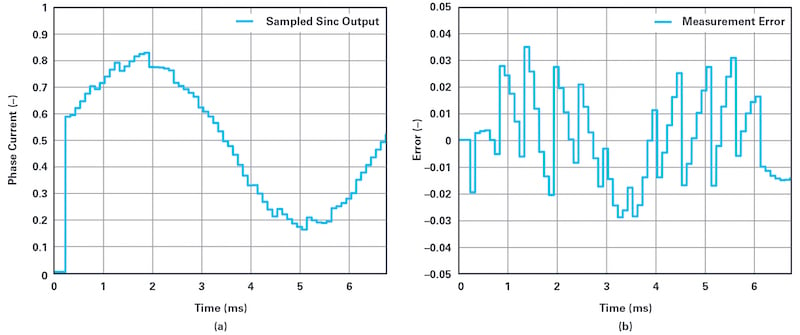
Figure 7. (a) Sampled output from the sinc filter. (b) Measurement error. Image used courtesy of Bodo's Power Systems.
It is clear the phase current measurement is highly distorted and would lead to poor control performance. Increased torque ripple and a need to reduce the bandwidth of the current control loop should be expected. If the measurement in Figure 7a is subtracted from the ideal measurement (Figure 5a), the error is obtained (see Figure 7b). The error is approximately 7% of the full-scale signal, which is very far from matching the expected 14 ENOB.
This sigma-delta measurement and aliasing scenario demonstrates a very common operating mode of sigma-delta-based current measurement and how it has led designers to conclude that sigma-delta ADCs are unsuited for motor drives. However, the example does not demonstrate the poor performance of the ADC itself. Rather, it demonstrates poor performance of the remaining signal chain because it is not properly set up for phase current measurement.
The ADC samples the input signal at several megahertz (typically 10 MHz to 20 MHz), and, with a decimation rate of 256, the sinc filter effectively removes the modulation noise. With such a high sampling rate the ripple component of the phase current is present in the filter output and that can become a problem in the downsampling stage of the signal chain (see Figure 1). If the ripple component is not sufficiently attenuated, and the motor control algorithm consumes current feedback at the PWM rate, the result is aliasing due to downsampling.
To avoid aliasing, the signal must be free of energy above half the sampling frequency, as per standard sampling theory. If the sigmadelta ADC output is downsampled to 10 kHz, any noise at 5 kHz or higher would fold into the measurement. As shown, there was plenty of 10 kHz switching noise left in the signal after the sinc filter. One option to attenuate the 10 kHz noise is to increase the decimation rate, but doing so would result in an unacceptably long group delay. A different approach is needed.
Improving Measurement Through Synchronization
The main problem with the antialiasing approach discussed in the previous section is illustrated in Figure 8. The output from the sinc filter is read at some instant uncorrelated to the switching component of the phase current. When the output is read, the filter delivers a weighted average of the input signal according to the impulse response. Sometimes this weighted average spans the low point of the switching waveform and sometimes it spans the highpoint. As a result, the signal used as feedback contains significant noise with frequencies from 0 Hz to half the PWM frequency.
A sigma-delta ADC samples continuously and the sinc filter outputs multiple measurements per PWM cycle (typically 10 to 20). Since each measurement spans 3 decimation cycles, the impulse responses overlap. For simplification, only three of these measurement/impulse responses are shown in Figure 8.
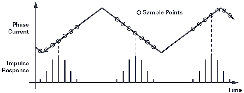
Figure 8. The impulse response is uncorrelated to the switching waveform. Image used courtesy of Bodo's Power Systems.
The source of the problem is that the impulse response is not locked to the switching component of current, which in turn is locked to PWM. The solution is to select the decimation rate so that there is a fixed integer number of decimation cycles per PWM period. For example, with a PWM frequency of 10 kHz, a modulator clock of 20 MHz, and a decimation rate of 200, there are exactly 10 decimation cycles per PWM period. With a fixed number of decimation cycles per PWM period, the impulse response is locked to PWM at all times and the measurement used for feedback is captured at the same point within the PWM cycle. The measurement of the phase current in this synchronization scheme is shown in Figure 9a.
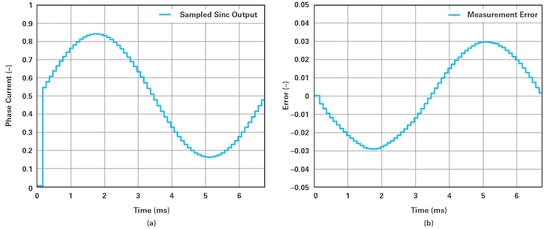
Figure 9. (a) Sampled output from the sinc filter when the impulse response is locked to PWM. (b) Measurement error. Image used courtesy of Bodo's Power Systems.
It is clear that synchronizing the impulse response to PWM has had a positive effect. The noise has been eliminated and, at first glance, the result seems similar to the ideal measurement in Figure 5a. However, when the sigma-delta measurement is subtracted from the ideal measurement, the result is the error signal in Figure 9b. The error magnitude is similar to the one shown in Figure 7b, but the frequency spectrum has changed. Now the error is a first-order harmonic that is equivalent to a gain error. The reason for this error pattern is illustrated in Figure 10.
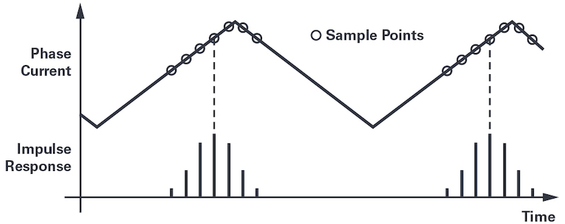
Figure 10. The impulse response is locked to a fixed point within the switching period. Image used courtesy of Bodo's Power Systems.
While the white noise error component has been eliminated, the signal is still distorted because the measurement is biased by the switching component. In Figure 10, notice how the sinc filter impulse response gives a weighted average around the peak of the switching waveform. Depending on the phase of the impulse response with respect to PWM, the size of the bias is limited only by the magnitude of the ripple current. As illustrated in Figure 3, the magnitude of the ripple component changes over a fundamental period, with the highest ripple at the peak of the fundamental current and the lowest ripple at zero-crossing. Because of this, the measurement error is a first-order harmonic component.
To get rid of the first-order harmonic measurement error, the impulse response must always be centered around the beginning or around the center of a PWM period where the phase current is exactly at its average value. Figure 11 shows the impulse response centered at the beginning of a switching period.
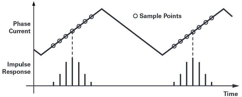
Figure 11. The impulse response is locked to the switching period and aligned to the ideal measurement point. Image used courtesy of Bodo's Power Systems.
Around this point the switching waveform is symmetrical, so by having an equal number of measurement points on either side, the ripple component averages out to zero around this point.
With the impulse response locked and centered around the instant of average current, the resulting measurement is shown in Figure 12a and the measurement error is shown in Figure 12b. As the ideally sampled measurement, the signal is free of both white noise and gain error.
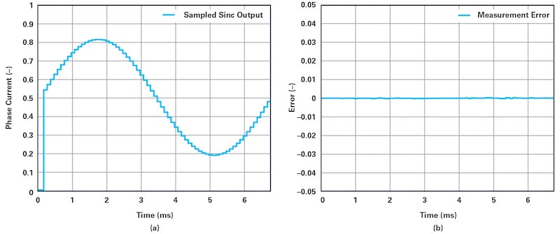
Figure 12. (a) Sampled output from the sinc filter when the impulse response is locked to PWM and centered around the instant of average current. (b) Measurement error. Image used courtesy of Bodo's Power Systems.
The presented results show that the quality of a sigma-delta measurement relies on much more than just the decimation rate. The common belief that increasing the decimation rate will result in higher ENOB is only true in the absence of aliasing. Controlling the filter update rate and phase with respect to the input signal is much more important than the decimation rate. As an example, compare Figure 7, which was based on a decimation rate of 256, and Figure 12, which was based on a decimation rate of 200. Lowering the decimation rate improved the measurement significantly.
Summary of Part 1
In summary, the conditions for an optimized sigma-delta-based phase current measurement are:
- The impulse response of a third-order sinc filter is 3 decimation cycles long, meaning it takes 3 decimation cycles for data to propagate through the filter.
- The impulse response of the filter must be centered around the instant of average current.
- 1.5 decimation cycles of the impulse response must be located before the instant of average current and 1.5 decimation cycles of the impulse response must be located after the instant of average current.
- The sinc filter generates multiple outputs during a PWM period, but only one of these outputs is used. The rest are ignored.
This concludes Part 1 of this article series. Part 2 will move on to propose a new sinc filter structure that is particularly suited for motor control applications and discuss how to best implement sinc filters on an FPGA. To verify the ideas discussed in the article series, Part 2 also presents several measurements performed on an FPGAbased, 3-phase servo drive.
References
- Jens Sorensen and Dara O’Sullivan. “A System Approach to Understanding the Impact of Nonideal Effects in a Motor Drive Current Loop.” Proceedings of PCIM Europe 2016.
- Jens Sorensen. “∑-Δ Conversion Used for Motor Control.” Proceedings of PCIM Europe 2015.
- Ahmet M. Hava, Russel J. Kerkman, and Thomas A. Lipo. “Simple Analytical and Graphical Methods for Carrier-Based PWM-VSI Drives.” IEEE Transactions on Power Electronics, January 1999.
This article originally appeared in Bodo’s Power Systems magazine.