Facebook
 Google
 GitHub
 Linkedin
IGCT – A Highly Efficient Device with Continuing Great Success in High Power Applications
This article compares the IGCT with IGBT and discusses its advantages of IGCT over IGBT in terms of power density as well as device and converter losses.
For reliable and efficient operation in high power applications, the Integrated Gate Turn-off Thyristor (IGCT) is the ideal device. The main advantage besides high reliability is the low device losses resulting in low system losses. In this article we compare IGCT and IGBT based 3-level converters with respect to device and system losses.
Since the end of the 1990s, the IGCT became the device of choice in applications where high power handling capability, low losses and high reliability are required. Typical applications are motor drives, interties, breakers and renewables. Reasons for this are the very low on-state losses provided by the thyristor structure, the negligible turn-on losses in the semiconductor and the high reliability of the device. The proven field experience in the aforementioned applications points out the IGCT as the ideal switch for the latest circuit topologies like modular multilevel converters (MMC) especially for highest power handling capabilities like in high-voltage DC current systems (HVDC).
Efficiency analysis of high-power semiconductors for converter ratings >5 MVA
Besides the high device reliability, the low device losses are the main advantage of the IGCT especially for applications in the range above 5 MVA. To demonstrate this, a loss comparison through simulation is presented between a converter equipped with IGCTs and a converter with IGBTs. The comparison was done using the ABB simulation tool SEMIS which is based on the PLECS software. All the semiconductor losses are calculated referencing datasheet conditions through lookup tables prepared by ABB to reflect the latest product specifications. A typical 3-level Voltage Source Converter (VSC) with diode Neutral Point Clamping (NPC) circuit is accounted in inverter mode as shown in figure 1, typically used in motor drives or wind generator converters.

Figure 1: SEMIS simulation circuits
In each circuit are applied the same DC voltage, switching frequency Fsw, power factor PF, device heat sink to ambient thermal resistance Rth and ambient temperature parameters for the IGCT and IGBT case, respectively. The comparison was done with ABB’s well-established 4.5 kV IGCT (5SHY 35L4520) and IGBT (5SNA 1200G450350) devices. Since the simulation accounts for one semiconductor per converter position as shown in figure 2 and having in mind the highest current capability of the IGCT compared with that of insulated IGBT modules, a scaled comparison of the losses was evaluated.

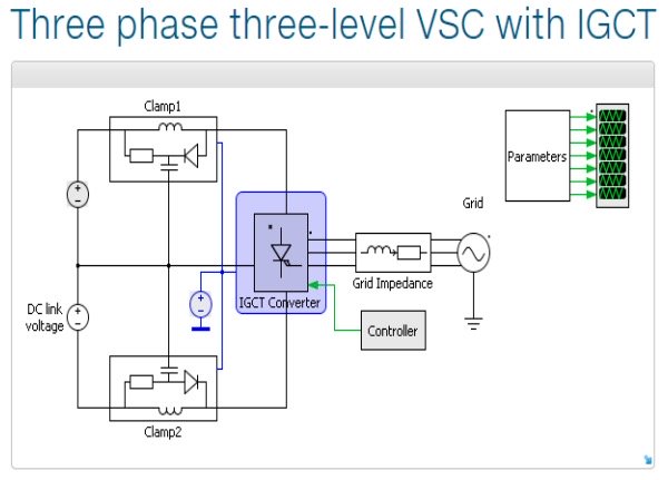
Figure 2: Thermal configuration of IGCT and IGBT based topologies
By simulating the clamp circuit operation, the losses on the clamp resistor dissipated for both upper and lower clamp of the 3-level IGCT topology were accounted for 2 options of the selected clamp inductor Li. Moreover, in the IGCT circuit the ABB press-pack diode 5SDF 20L4520 optimised for IGCT application was chosen for the free-wheeling diode (FWD), NPC and clamp positions. For the NPC position in the IGBT based converter the standard ABB product 5SLD 1200J450350 was used. To distinguish the thermal configuration of the IGCT and IGBT based converter concepts, the following factors were accounted: The IGCT packaging concept is that of a press-pack device with double side cooling while with the IGBT we have an insulated module with only the baseplate contacting the heat sink area. The FWD part is integrated in the IGBT module in the same package whereas for the asymmetric IGCT selected for this simulation, a separate press-pack FWD was used with its own double side cooling concept (figure 2).

Table 1: IGCT and IGBT PEBB operating conditions
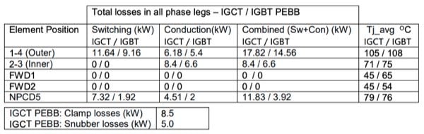
Table 2: IGCT and IGBT PEBB semiconductor losses
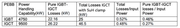
Table 3: Performance comparison
The operating conditions of the Power Electronic Building Block (PEBB) and the IGCT / IGBT simulation results are presented in tables 1 to 3. They are calculated based on a three phase 3-level topology with 12 controlled semiconductors (IGCT and IGBT, respectively) and 12 diodes in free-wheeling position and 6 diodes in NPC position. It is clear that the power density achieved with single devices per converter position is double in the case of the IGCT design. A high power factor PF was selected close to 1 to minimise the losses of the free-wheeling diodes. In any case for power factors in the range of 0.85 to 0.95 the contribution of these diodes to the overall losses for inverter mode is minimal, i.e. in the range of few hundreds of watts in total at maximum. Similar considerations apply for the switching losses of the controlled element in position 2, be it an IGBT or an IGCT. The switch in that position experiences virtually no switching losses accounting for its duty cycle which is continuously conducting and commutates to 0 current under zero voltage. This is also due to the NPC diode operation applying 0 voltage across position 2 of an active switch. The current of devices in position 2 exhibits a smooth continuous shape. The effect of a highly inductive power factor and increased switching frequency results in appearance of very few and negligible switching losses. Figure 3 shows scope waveforms of IGCT2 taken during the simulation which indicate this behaviour.

Figure 3: IGCT2 switching losses (a) PF=0.95, Fsw=450 Hz, (b) PF=0.8, Fsw=750 Hz
Proportionally the losses in the semiconductors are much lower in the case of the IGCT converter and even with the estimation of the additional losses in the clamp circuit with the higher clamp inductor Li option they are still lower compared to the IGBT based converter. It is also interesting to observe the pure losses in the controlled semiconductors as a ratio to the input power drawn from the DC side. This figure shows clearly the performance advantage of the IGCT.
Conclusion
The IGCT is proven over the years as the preferred device for high power applications especially above 5 MVA. Using the ABB SEMIS simulation tool a comparison was made between IGCT and IGBT based concepts for a common 3 level NPC VSC circuit. It is evident from the results that the IGCT allows for higher power density without the need of paralleling devices. At the same time it is resulting in proportionally lower device and converter losses than IGBT based configurations at comparable operating conditions. From these facts the system designer benefits in many ways. The higher power density allows for smaller converter footprint and simplicity on the semiconductor control circuit. The lower losses provide better performance and operational cost saving. ABB has a long history of evolution for this semiconductor element and is currently developing next generation technologies which will allow even higher capabilities.
About the Authors
Vasilis Kappatos worked as the Senior Application Engineer for Power Semiconductors at ABB Switzerland since April of 2014. Now, he works as the Bid and proposal engineer for MV drives since March 2018. He is highly skilled in the field of photovoltaics, solar energy, as well as electrical engineering field. He earned his Diploma as a Technologist Electrical Engineer at the Technological Education Institute of Piraeus where he was an apprentice at the industrial automation switchboards design and implementation department. He then earned his Diploma in Electrical and Computer Engineering, Power Systems, Power Electronics - Automation at the University of Patras.
Sven Klaka works as the Technology and Product Manager for Semiconductors at ABB Switzerland since May 2008. He is skilled in the field of marketing and key account management. He earned his Diploma in Physics at the Technical University of Braunschweig as well as his Engineering Doctorate in Electrical Engineering at the same university.
Christian Winter works as the Global Product Manager of BiPolar Semiconductor Products at ABB Switzerland Ltd. – Semiconductors, Lenzburg, Switzerland. He is responsible as product manager for the BiPolar product portfolio consisting of the three lines: diodes, thyristors and IGCT / GTO, with production sites in Lenzburg and Prague. Developing, deciding and consolidating the product portfolio, the roadmap, the budgets of the corresponding development projects and the marketing strategies of the product lines. He earned his Höhere Technische Lehranstalt (HTL) in electrical engineering at the University of Applied Sciences and Arts Northwestern Switzerland or FHNW.
Madhan Mohan works as the Proposal Engineer at ABB since June 2015. He earned his Bachelor's Degree in Electrical and Electronics Engineering at the Thangavelu Engineering College located in Nadu, India.
This article originally appeared in the Bodo’s Power Systems magazine.