Facebook
 Google
 GitHub
 Linkedin
GaN Technology: Now With 2200 V Rating
The release of 2200 V PowiGaN technology marks the next major step in high-voltage GaN power conversion. Power supply engineers grappling with the challenge of higher power density in EVs, AI data centers, BESS, and photovoltaic converters (among others) will be able to stop designing around the voltage-limit problem inherent in conventional GaN switches.
This article is published by EEPower as part of an exclusive digital content partnership with Bodo’s Power Systems.
The release of 2200 V PowiGaN™ technology marks the next major step in high-voltage GaN power conversion. Power supply engineers grappling with the challenge of higher power density in EVs, AI data centers, BESS, and photovoltaic converters (among others) will be able to stop designing around the voltage limit problem inherent with conventional GaN switches.

Image used courtesy of Freepik
GaN-on-silicon HEMTs have a maximum commercially available operating voltage of 900 V. GaN-on-sapphire is the technology differentiator employed to create PowiGaN™ switches – a proprietary approach to GaN switches developed and owned by Power Integrations. The potential effect of 2200 V GaN was recently described by Roy Dagher, PhD, Technology & Market Analyst, Compound Semiconductors at Yole Group, as follows: “GaN’s voltage ceiling has kept it out of the main power path, ceding that ground to SiC. A 2200 V rating changes this, giving margin for single-stage topologies and future-proofing emerging 1500 V data center and EV designs…”
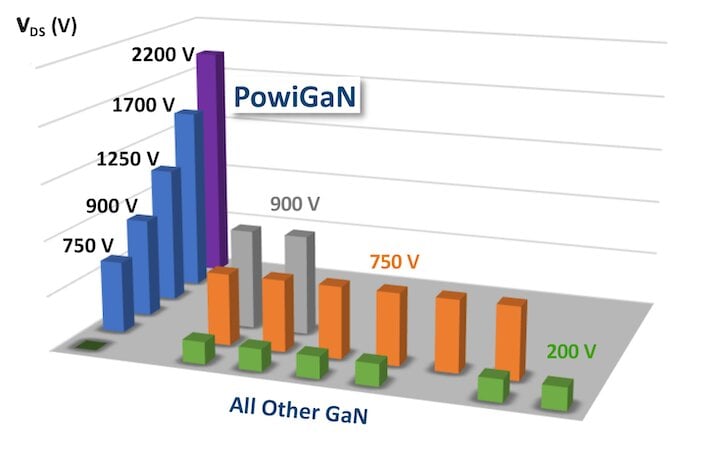
Figure 1. A comparison of the VDS rating of different lateral GaN power switch technologies available in the market today. PowiGaN uses a GaN-on-sapphire process to achieve high-voltage devices, whereas the other GaN in the market employs GaN-on-silicon. Image used courtesy of Bodo’s Power Systems [PDF]
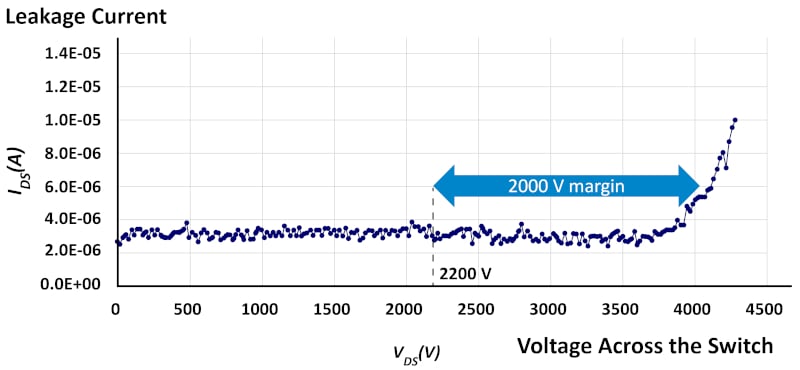
Figure 2. Leakage current (IDS) measured across a 2200 V PowiGaN switch. Note the substantial margin (>2000 V between rated voltage and rise in leakage current), which demonstrates the robust nature of the barrier at rated voltage. Increasing leakage margin is a key constituent in achieving high reliability (PowiGaN cascoded-HEMT technology has a FIT number of less than 1). Image used courtesy of Bodo’s Power Systems [PDF]
The insulating nature of sapphire substrate enables a markedly different high voltage performance compared to silicon. This in turn leads to an epitaxy-substrate boundary that can support much higher voltages – significantly in excess of the 2200 V described in the title. Not only does this allow high-voltage GaN devices to be created, but it also allows for the addition of substantial margin (more than 2000 V) above this rated voltage (see Figure 2).
The Cascode Advantage – Robust Operation, Simplified Control, Higher Efficiency
Moving PowiGaN switch technology into a cascode arrangement also overcomes GaN sensitivity with respect to gate voltage. A low-voltage silicon MOSFET is paired with the normally-on PowiGaN HEMT to provide a normally-off (enhancement mode) switch with a robust gate structure that is easy to drive and very reliable. This increased gate drive robustness and reliability factors into the long lifetime (1 FIT) noted above and has resulted in automotive qualification for PowiGaN devices.
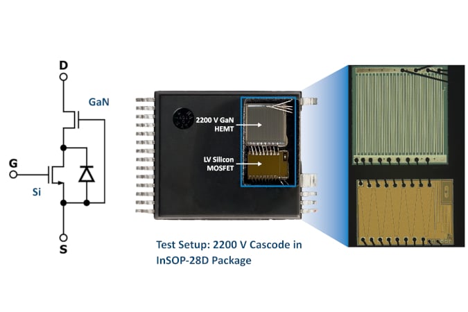
Figure 3. Cascode structure – the GaN HEMT is allowed to operate in its natural depletion mode and provides the low RDS(ON) and voltage isolation that characterizes GaN switches, while the low-voltage, low RDS(ON) series MOSFET provides robust gate-drive inversion for the HEMT to create a normally-off (enhancement mode) switch. Image used courtesy of Bodo’s Power Systems [PDF]
At higher power levels, vertically stacked die architectures will be necessary to create a practical cascode structure which will be married to the higher voltage GaN devices; the approach is potentially stackable into systems in the order of 20 kW, subject to topology, frequency, cooling and paralleling assumptions.
High Voltage GaN Simplifies Design Challenges
In the 800 V Bus (and higher) space, bias supplies typically employ a flyback converter that must withstand high voltage. The worst-case voltage stress seen by the power switch can be approximated to the sum of three main sources. The maximum bus voltage (typically 10 % higher than the headline value) is the first and largest contributor.
The second contribution is from the output voltage reflected back onto the primary side of the converter (termed VOR) – this is the output voltage multiplied by the transformer turns ratio and can be in the order of 200 V for a (commonly required) 48 V output. The third voltage stress adder for the primary switch is caused by leakage inductance. Leakage inductance is the magnetic flux in the flyback transformer that is not coupled to the secondary side.
When the transformer turns off, magnetizing inductance energy (the energy that is coupled to the output windings) is commutated and discharged to the output. Leakage flux has nowhere to go. Leakage current that has built up during the primary switch-on time cannot fall instantly to zero. Instead, the energy trapped in the leakage flux is discharged as a high-voltage spike that appears on top of the primary rail at the moment the primary switch turns off.
The leakage spike can be in the order of 80 - 150 V depending on the transformer design and the size of the snubber circuit added to clamp it. A stylized flyback primary switching waveform with these three voltage elements identified is shown in Figure 4. The combination of these voltages describes the voltage stress on the primary switch.
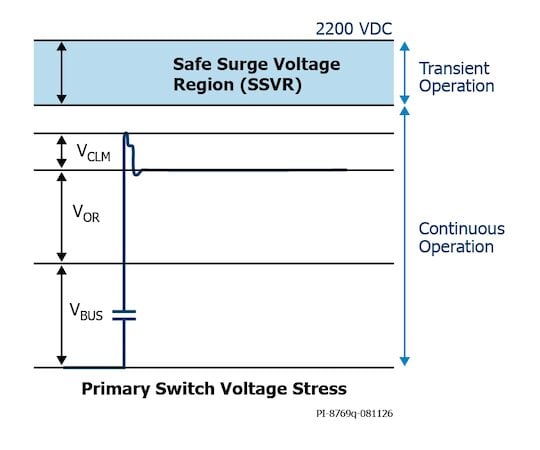
Figure 4. Simplified primary switch voltage waveform for a flyback converter showing the voltage stress on the power switch, which is set by bus voltage (VBUS), reflected voltage (VOR), and the amplitude of the leakage inductance clamp voltage (VCLM). The sum of these three elements describes the withstand voltage the switch must be able to support in normal operation. The voltage must remain below the Safe Surge Voltage Region (SSVR) during continuous operation. In the SSVR, recoverable RDS(ON) shift begins to occur, and this voltage region is reserved for short duration rather than continuous operation. A typical design margin (perhaps 20 %) is applied to the maximum stress seen on the switch in normal operation and is compared to the switch voltage rating that bounds the top of the SSVR. Image used courtesy of Bodo’s Power Systems [PDF]
For the resonant half-bridge that typifies higher power conversion, the maximum primary-switch voltage-stress is given by:
VDS(PEAK) = VBUS + VCLM + VTRANSIENT + VRING
Where:
VDS(PEAK): Maximum voltage across each primary switch
VBUS: Maximum DC input voltage to the half-bridge circuit
VCLM: Clamp voltage
VTRANSIENT: Voltage overshoot on the primary switch caused by COSS
VRING: Oscillatory (ringing) component caused by LC resonance of parasitic elements
The half-bridge circuit imparts less voltage stress than the flyback, but for a 1500 V BUS application, the 2200 V rating of the new PowiGaN process is ideal.
VOR Is Limited by the Voltage Rating of the Secondary Side Rectifier
A significant challenge of high-efficiency flyback power supplies is designing a practical circuit that operates within the drain-to-source voltage limit of the logic-level SR MOSFET (or GaN) typically used. A device limit of 150 V is typical. To limit the voltage stress on the SR MOSFET, designers can opt to increase the turns ratio of the transformer. This will increase VOR (and hence voltage stress on the primary switch). A similar argument can be made for voltage stress on the SR MOSFETs in a resonant half-bridge circuit.
The 2200 V rating demonstrated for PowiGaN provides the engineer with more design freedom to balance the voltage stress between the primary switch and the secondary-side SR MOSFET by adjusting the turns ratio of the transformer.
Switching Frequency Benefits With PowiGaN Compared to SiC
800 V systems for EV and data center market spaces are already embracing GaN despite the availability of SiC devices and the voltage limitations of existing (750 V) high-power GaN switches. In both these application types, minimizing size is a critical requirement. Higher switching frequency results in a smaller switching transformer and is a first-order effect. Figure 5 describes the relationship between switching frequency and the cross-section (Ae) of the switching transformer.
While SiC devices can switch at frequencies up to 500 kHz, device capacitances mean that switching frequency for practical SiC-based converters is often constrained below this range. GaN devices exhibit much lower capacitances for equivalent on-resistance (see Table 1), making them ideal for higher frequency switching. Resonant (soft) switching means that the EMI effects of a higher switching frequency are minimized. Power converters up to 20 kW are able to use a switching frequency in the 500 kHz to >1 MHz range.
The relationship between switching frequency and transformer cross section for a Half-Bridge power supply is described in the following formula, where Ae equals the effective core cross-sectional area (m²) and f = switching frequency (Hz), BPK = peak flux density (T), which is typically limited to less than 300 mT (3000 Gauss), Vpri = DC voltage applied to the transformer primary, N = primary turns
\[A_{e}=\frac{V_{pri}}{4NB_{pk}f}\]
The lower transformer cross-section translates to lower power converter height, especially when planar magnetics are utilized. The effects of WBG switch parasitic effects on resonant circuit performance can only be summarized here, but they demonstrate why design engineers looking for the highest efficiency and smallest size are already embracing GaN technology even when low-voltage capability necessitates the use of multiple series-connected HEMTs.
Table 1. Comparison of parasitic circuit elements for different WBG technologies.
| Parameter | 650-V GaN FET | 650-V SiC MOSFET |
| CISS | 200-1000 pF | 1000-5000 pF |
| COSS | 20-200 pF | 100-1000 pF |
| CRSS | 1-20 pF | 10-100 pF |
| QG | 5-20 nC | 20-100 nC |
For a high-frequency resonant half-bridge, CISS controls gate charge QG and therefore gate charging current from the driver; QG controls gate-driver loss and indirectly affects switching speed. CRSS controls switching transition loss – less important in resonant circuits. COSS controls the resonant commutation current and is critical for light-load efficiency (very important in EV applications).
\[\frac{1}{2}L_{r}I^{2}_{r}>C_{OSS}V^{2}_{BUS}\]
where Ir is the resonant commutation current
At frequencies above 500 kHz, minimizing QGD and COSS can be as important as, or more important than, RDS(ON) conduction losses.
Higher Efficiency from a 2200 V Cascode in Half-Bridge Applications
Efficiency is critical in many emerging applications. In half-bridge cascode-based PowiGaN switches offer lower loss in 3rd quadrant operation than can be achieved with conventional GaN devices. A summary of this is shown in Figure 5.
Application Space for High Voltage GaN Switches
Practical circuit testing shows that the 2200 V process is robust – exhibiting resistance to charge-trapping, dynamic RDS(ON), and current collapse effects. The technology is ready to be deployed in main power switching circuits and auxiliary power supplies in half-bridge and flyback configurations, respectively.
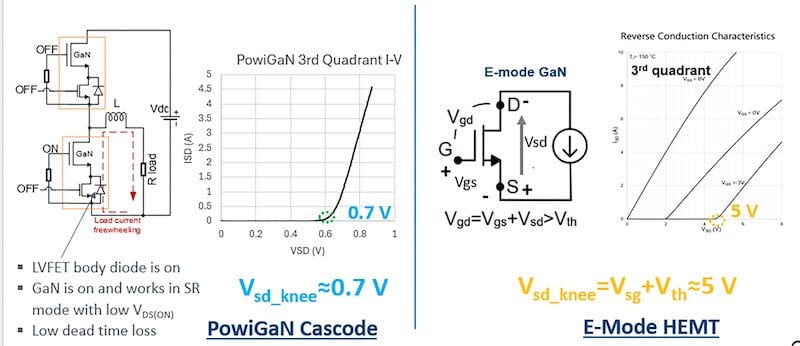
Figure 5. In a half-bridge application, during 3rd quadrant (diode conduction) operation, the normally-on PowiGaN cascode presents a lower voltage drop compared to conventional Emode devices, increasing circuit efficiency. Image used courtesy of Bodo’s Power Systems [PDF]
SiC owns the switching market space above 800 V today. However, there are applications already in place that require the unique capabilities of high-voltage GaN devices. SiC MOSFETs are limited to applications where small size is not a requirement.
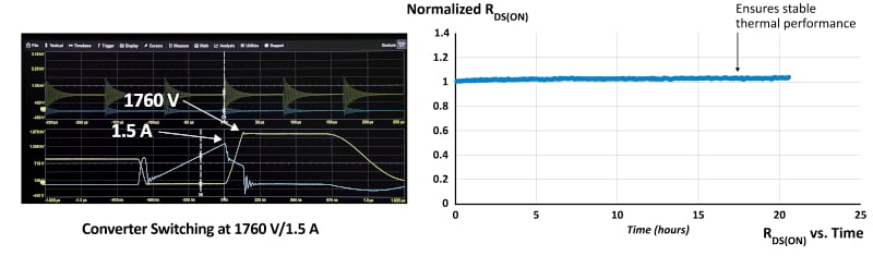
Figure 6. Dynamic High Temperature Operating Life (D-HTOL) testing of 2200 V PowiGaN showing normalized RDS(ON) measured in a flyback architecture shows no significant dynamic RDS(ON) effects in the GaN switch. Image used courtesy of Bodo’s Power Systems [PDF]
This is because SiC devices have a relatively low maximum switching frequency (typically described as being in the order of 250 kHz). Higher frequency would allow a move to smaller magnetics, so for applications such as On-Board-Charging (OBC) in EVs and AI data centers, the benefits are readily apparent due to the very limited space available. Indeed, data centers are already embracing GaN switches, where multi-level architectures are currently being employed to overcome the voltage limits of conventional devices (as shown in Figure 7).
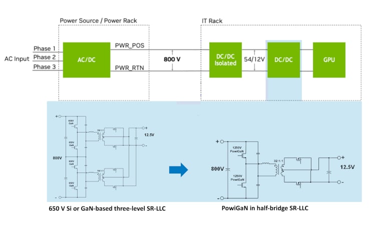
Figure 7. To meet the power distribution challenges of AI data centers, multi-level architectures are being employed for 800 V systems. The move to 1500 V systems to meet ever-increasing higher power requirements has already been discussed. High-voltage PowiGaN-based devices allow the move to a simplified single-level switching architecture – reducing circuit cost, design complexity, and solution size. Image used courtesy of Bodo’s Power Systems [PDF]
Higher voltage allows more power, so for data centers, 1500 V bus architectures are being actively pursued. To meet derating requirements, main power switches will need the 2200 V rating.
Automotive manufacturers in the US and EU are exploring 1200-1500 V for commercial vehicle charging and are sizing their power delivery systems accordingly. In China, BYD has decided to push for super-fast battery charging and is proposing a 1 MW charger to deliver ultra-fast charging for electric vehicles using their Super e-Platform.
Higher EV charging speed will require an increased voltage bus, and 1150 V has already been identified as a new standard. This voltage level is not fully supportable with even the 1700 V PowiGaN – especially for auxiliary power systems running from flyback converters. 2200 V will be required to support this environment. Finally, HVDC transmission and utility-scale Battery Energy Storage Systems (BESS) already employ a 1500 VDC rail architecture and will benefit from higher power density.
Industry is replete with SiC manufacturing capacity today, which has lowered pricing for the technology and allowed its adoption in an increased range of applications. Because of this, higher-voltage GaN will initially be deployed in areas that will significantly benefit from the smaller size and enhanced efficiency that the technology provides. In the long term, high-voltage GaN can offer a compelling path where switching frequency, architecture simplicity, and power density will outweigh the maturity and current pricing of SiC.
2200 V PowiGaN will enable the design of smaller, more efficient, and robust power converters from flyback auxiliary power up to 20 kW resonant half-bridge circuits. The introduction of vertical GaN - still some way off- may also provide a pathway into the highest power switching applications (> 20 kW), but that is a discussion of another time.
This article originally appeared in Bodo’s Power Systems [PDF] magazine.