Facebook
 Google
 GitHub
 Linkedin
GaN — Assuring Price, Volume and Security of Supply
(Performance and Reliability are Expected). Gallium nitride is still regarded as a new technology by many. Although GaN is now widely used in chargers and adapters for mobile phones delivering efficiency and power density benefits, other sectors, such as automotive, LED drivers, renewable energy, consumer audio, and phone handsets, are only just realizing that GaN’s superior switching performance is suitable for their applications too.
Of course, there are early adopters but before the market switches en-masse, they need to be confident that commercial factors, as well as engineering concerns, have been considered too. Innoscience, the largest 8-inch GaN-on-Si device manufacturer, is addressing these concerns with proven technology, rugged, qualified processes, and massive capacity.
Innoscience was founded in December 2015 with the aim of creating the world’s largest manufacturing company fully focused on 8in GaN-on-Si technology. From the very beginning, Innoscience executives understood that for GaN technology to become ubiquitous in many markets, performance and reliability - although vital - were only the starting point. Before GaN could become widely adopted, customers would have three additional key demands. First, GaN technology devices must be affordable, as the industry is not willing to pay a big premium. Second, a large manufacturing capacity is necessary in order to deliver large volumes and absorb fluctuations in demand. Third, customers require security of supply, allowing them to develop their products and systems using the new GaN devices without worrying about possible production discontinuations and shortages.
Remember that the emergence of GaN has coincided with one of the most brutal periods of global chip shortages ever experienced by the electronics industry.
Therefore, Innoscience understood that only by focusing on 8in GaN-on-Si technology, dramatically scaling up GaN-on-Si device manufacturing and controlling its own production fabs, would it be possible to meet the requirements of the electronic industry (price, volume and security of supply).
Innovative Technology
But just as performance and reliability must always be proven before any other concerns, let’s first look at the technology, which Innoscience has developed together with its trusted international partners.
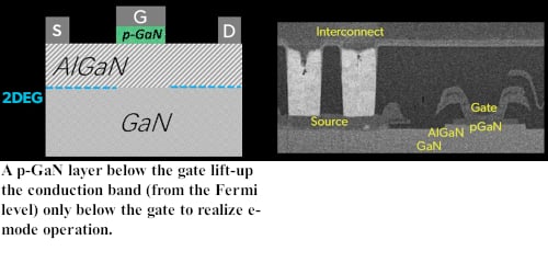
Figure 1. A p-GaN layer, grown on top of the AlGaN barrier, forms a Schottky contact with the p-GaN layer resulting in normally-off/e-mode operation. Image used courtesy of Bodo’s Power Systems
Power semiconductor engineers demand devices that show a normally-off operation - i.e. no current conduction when the transistor’s gate is set at 0V. Since the natural form of GaN HEMTs (High Electron Mobility Transistors) is normally-on (so-called depletion mode), special drivers must be placed in a cascode package solutions to realize normally-off operation. However, Innoscience’s GaN HEMTs are intrinsically normally-off (enhancement mode) devices. Normally-off operation is realized by growing a p-GaN layer on top of the AlGaN barrier, forming a Schottky contact with the p-GaN layer (Figure 1). This increases the potential in the channel at the equilibrium, resulting in normally-off/e-mode operation.
Low Specific RDS(on)
A key parameter for defining device performance is the specific RDS(on), the on-resistance per unit area. The lower the specific RDS(on), the smaller a device can be made, enabling more devices per wafer and lower device cost.
Innoscience has developed a proprietary strain enhancement layer technology, which consists of the deposition of a specific layer after the gate stack definition. The stress modulation created by the strain enhancement layer induces additional piezoelectric polarizations which causes the 2DEG density to increase reducing the sheet resistance by 66%. Since the strain enhancement layer is deposited after the gate formation, it only affects the resistance in the access region and it does not impact other device parameters such as threshold and leakage etc.
Therefore, Innoscience’s GaN-on-Si e-mode HEMTs show very low specific on-resistance. Because Innoscience has optimized both epitaxy as well as device process technology, the (dynamic) RDS(on) does not increase over the full temperature and voltage range, suiting it for power switching applications.
High Throughput, High Yield
Silicon technology has been in mass production for 50 years. Silicon device manufacturers supported by the toolmakers, have optimized their process in terms of throughput and quality in order to utilize every available mm silicon wafer area and to produce as many wafers as possible. Innoscience is leveraging all this experience and expertise. The company is committed to 8in wafer processing, and its two fabs are equipped with the latest equipment, including ASML scanners. Process flows are similarly optimized. Because Innoscience is a fully-integrated company, controlling all manufacturing stages from device design, through EPI and wafer processing to failure & reliability analysis - i.e. full GaN-on-Si production - the company achieves both high wafer and device yield. It also means that new products can be designed and in test within 3 -6 months and be ready for mass production within just 6 months.
Today, Innoscience produces more than 10,000 8in GaN-on-Si wafers every month; this will increase to 70,000 wafers per month by 2025. The first Innoscience fab is already qualified for ISO 9001 and the IATF 16949:2016 certification for automotive use, and the GaN HEMTs are qualified to the JEDEC standard as well as Innoscience performs more advanced reliability tests to test their devices.

Figure 2. Innoscience has developed a strain enhancement layer technology resulting in low RDS(on). Image used courtesy of Bodo’s Power Systems
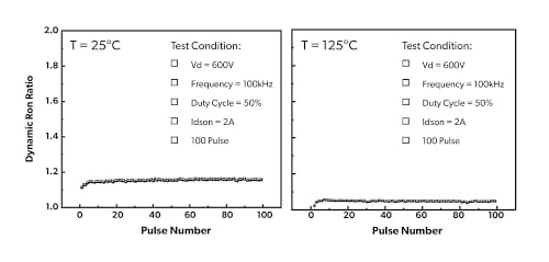
Figure 3. Innoscience’s GaN devices show no appreciable drift in RDS(on) over the full temperature and voltage range. Image used courtesy of Bodo’s Power Systems
Product Mix
Uniquely for a GaN company, Innoscience offers devices that cover low (30-150V) and high voltage (650V) ranges. Innoscience’s GaN HEMTs (InnoGaN) are available from 30-150V in chip-scale packages (csp) measuring 2x2mm to 2.2x3.2mm with RDS(on) down as low as 5.5mΩ (typ). 650V parts in DFN and wafer-scale feature RDS(on) levels as low as 106mΩ (typ). Innoscience GaN HEMTs are being used in USB-PD chargers up to 120 W and in LLC converters. They are to be found inside data center power supply racks. In the near future, they will be found inside automotive applications including LiDAR systems, on-board chargers (OBC), 48-12V DC/DC step down converters and high voltage 650/900V DC/ DC converters. Innoscience InnoGaN parts outperform traditional silicon FETs in LED lighting. Astonishingly, Innoscience’s 40V bidirectional part is the first time in the world that GaN HEMTs can be used inside a smartphone, reducing the size of the over-voltage protection (OVP) unit inside the battery management system (BMS) by at least 50%.
Conclusion
By combining world-class technology, state-of-the-art processing technology, and the world’s largest 8in GaN-on-Si capacity, Innoscience is answering both engineering and commercial challenges, enabling designers working in all market sectors to benefit from the proven performance benefits with no cost penalty.
This article originally appeared in Bodo’s Power Systems magazine.