Facebook
 Google
 GitHub
 Linkedin
CMOS Flip-Flops: JK, D and T-Type Flip-Flops
Learn how the CMOS JK flip-flop device and its derivations work.
The SR flip-flop is the fundamental memory element. The JK flip-flop – developed for special applications – started from it and defeated the difficulty of a forbidden input combination. Variations to the JK flip-flop produce the master-slave D, and T flip-flops.
The JK Flip-flop
The following discussion assumes positive logic – logic 1 with active high inputs.
The letters J and K come from the initials of its inventor, Jack Kilby.
The JK flip-flop eliminates the uncertainty in the truth table of the SR flip-flop. Figure 1 shows a building block of the JK flip-flop.
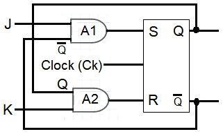
Figure 1. A JK flip-flop.
The JK flip-flop comprises an SR flip-flop with two added AND gates – A1 and A2. A1 receives the data input J and the output Q̅. A2 receives the data input K and the output Q.
Table 1 shows the four possible combinations for J and K. Since each grouping of J and K has two possible states of Q, the table has eight rows. The table also displays the S and R inputs calculated for each combination of inputs. The Qn+1 column comes from the S and R inputs and the truth table for the SR flip-flop. The last column highlights the final condition of Qn+1.
|
Jn |
Kn |
Sn |
Rn |
Qn |
Complement |
Qn+1 |
Comment |
|
0 |
0 |
0 |
0 |
0 |
1 |
0 |
No change of state |
|
0 |
0 |
0 |
0 |
1 |
0 |
1 |
|
|
0 |
1 |
0 |
0 |
0 |
1 |
0 |
Output = 0 |
|
0 |
1 |
0 |
1 |
1 |
0 |
0 |
|
|
1 |
0 |
1 |
0 |
0 |
1 |
1 |
Output = 1 |
|
1 |
0 |
0 |
0 |
1 |
0 |
1 |
|
|
1 |
1 |
1 |
0 |
0 |
1 |
1 |
Complement (Toggle) |
|
1 |
1 |
0 |
1 |
1 |
0 |
0 |
Table 1. The truth table for the JK flip-flop.
The truth table of table 2 is a summary of table 1.
|
Jn |
Kn |
Qn+1 |
|
0 |
0 |
Qn (No change) |
|
0 |
1 |
0 |
|
1 |
0 |
1 |
|
1 |
1 |
Complement (Toggle) |
Table 2. A summary truth table for the JK flip-flop.
We can see that the truth table is similar to the one corresponding to the SR flip-flop, except for the inputs Jn = logic 1, Kn = logic 1 where the output Qn+1 changes state (If it was logic 0 it goes to logic 1, and if it was logic 1 it goes to logic 0), eliminating the ambiguity.
It is essential to observe that these outputs occur when applying a clock pulse as discussed in the previous article.
An Alternative Building Block for a JK Flip-flop
Figure 2 shows another building block for a JK flip flop.
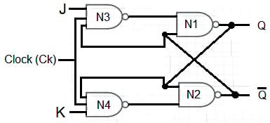
Figure 2. An alternate building block for a JK flip-flop.
This configuration uses the building block for the SR flip-flop but adds an input terminal to the NAND gates N3 and N4, providing feedback from the N1 and N2 outputs.
There is, however, a problem called the race-around condition related to the fast propagation speed of pulses in integrated circuits. This situation can produce ambiguous values at the outputs if the clock remains high for a sufficient amount of time. Delay lines in series with the feedback connections solve the problem, but this is not practical, and there are better solutions.
When the width of the pulse clocking the flip-flop is larger than the flip-flop's propagation delay, the change in state at the output is not dependable. The propagation delays are typically minimal, and the possibility of a race-around condition is pretty high.
JK Flip-flop with Preset and Clear Inputs
It is frequently required to clear a flip-flop to a logic 0 state (Q = 0) or preset it to a logic 1 state (Q = 1).
Two additional inputs to the NAND gates N1 and N2, in Figure 3, set the initial state of the JK flip-flop.
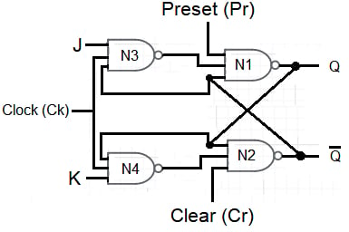
Figure 3. A JK flip-flop with preset and clear inputs.
The clear operation makes the output Q go to logic low. Achieving this goal requires setting the clear input Cr = logic 0 and the preset input Pr to logic 1. When Cr = logic 0, the output of N2 is Q̅ = logic 1, back-fed to an N1 input. If Ck = logic 0, the output of N3 is logic 1. Under these circumstances, all inputs to N1 are logic 1, and its output Q = logic 0.
To set the output to logic high, the clear input Cr = logic 1, the preset input Pr = logic 0 and then the output of N1 is Q = logic 1. Examining the rest of the circuit, we see that Q = logic 1 goes back to an N2 input and, since Ck = 0, the output of N4 is logic 1. Therefore, all inputs to N2 are logic 1, and its output is Q̅ = logic 0, as expected.
The preset and clear data are not synchronized with the clock but applied between clock pulses, i.e. when Ck=0.
To enable the flip-flop, keep the inputs Pr and Cr in logic 1 before the next pulse appears. Inputs Pr = Cr = logic 0 lead to an indeterminate state.
Table 3 shows this device's truth table.
|
Ck |
Pr |
Cr |
Jn |
Kn |
Qn |
Qn+1 |
|
|
Preset |
0 |
0 |
1 |
X |
X |
1 |
|
|
Clear |
0 |
1 |
0 |
X |
X |
0 |
|
|
Indeterminate |
0 |
0 |
0 |
X |
X |
- |
- |
|
Enable |
1 |
1 |
1 |
0 |
0 |
Qn |
|
|
1 |
1 |
1 |
0 |
1 |
0 |
||
|
1 |
1 |
1 |
1 |
0 |
1 |
||
|
1 |
1 |
1 |
1 |
1 |
Complement (Toggle) |
X = any value
Table 3. The truth table for a JK flip-flop with preset and clear inputs.
Note that the “Enable” section of table 3 matches the outputs shown in table 2.
The Logic Symbol for a JK FLIP-FLOP with Preset and Clear Inputs
Figure 4 shows the logic symbol for a JK flip-flop with preset and clear inputs.
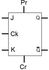
Figure 4. The logic symbol for a JK flip-flop with preset and clear inputs.
JK Master-Slave Flip-Flop
It is interesting to analyze the JK master-slave configuration because this is one way to get over the race-around condition.
Figure 5 shows a cascade of two JK flip-flops. The first flip-flop is the master and the second one is the slave. The master's outputs feed the slaves' inputs, and the slave's outputs feed the master's inputs.
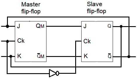
Figure 5. A JK master-slave flip-flop.
The clock to the slave flip-flop is the complement of the clock to the master flip-flop.
A master-slave flip-flop is pulse-triggered. The clock pulse Ck = logic 1 enables the master flip-flop and disables the slave flip-flop. Consequently, the master flip-flop changes state – following the JK flip-flop truth table shown in table 2 – but the slave flip-flop cannot, keeping Q constant when Ck=logic 1 and hence, avoiding the race-around trouble.
The clock pulse Ck = logic 0 disables the master flip-flop and enables the slave flip-flop. Thus, the slave flip-flop changes state as per the logic states at its J and K inputs.
The master flip-flop transfers its contents to the slave flip-flop, and the disabled master flip-flop acquires new inputs without affecting the output.
To summarize, the output Q does not change when Ck= logic 1 while QM follows the inputs according to the JK flip-flop truth table for Ck= logic 1; when the pulse ends, Q changes depending on the value of QM.
D (Delay) Flip-Flop
This flip-flop has a single input (D) and works so that the information present at the input is transferred to the output Q when a clock pulse appears, functioning as a 1-bit delay device. Table 4 shows its truth table.
|
Dn |
Qn |
Qn+1 |
|
0 |
0 |
0 |
|
0 |
1 |
0 |
|
1 |
0 |
1 |
|
1 |
1 |
1 |
Table 4. The truth table for the D flip-flop.
We can see in Table 4 that the input is transferred to the output when the clock pulse appears, regardless of the previous state of the output. That is why a reduced truth table can be made (Table 5).
|
Dn |
Qn+1 |
|
0 |
0 |
|
1 |
1 |
Table 5. A summary truth table for the D flip-flop.
One way of implementing a D flip flop is by adding an inverter to the JK flip-flop so that input K is the complement of input J, as shown in Figure 6.
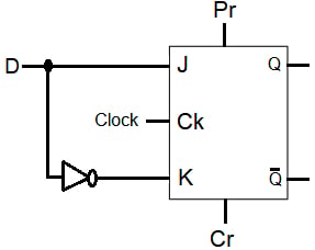
Figure 6. A D flip-flop.
We can deduct the D flip-flop truth table of Table 5 from the JK truth table in Table 2.
Another way of implementing a D flip-flop is by replacing the JK flip-flop in Figure 6 with an SR flip-flop, as shown in Figure 7. With this configuration, it also works as a latch.
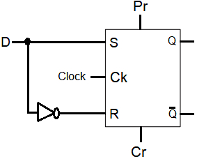
Figure 7. Another configuration for a D flip-flop.
In this configuration, S and R can never have the same logical state, making it impossible for the ambiguous state S = S = logic 1, fulfilling the truth table in Table 5.
Figure 8 shows the logic symbol for the D flip-flop.
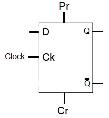
Figure 8.The logic symbol for a D flip-flop.
T Flip-Flop
This flip-flop (called T for "toggle"), like the D flip-flop, receives the information from a single input and is helpful to build logical arithmetic units.
The T flip-flop changes state with each clock pulse when its input T is logic high. If T = 0, there is no change of state at the output.
Table 6 shows the truth table for the T flip-flop.
|
Tn |
Qn |
Qn+1 |
|
0 |
0 |
0 |
|
0 |
1 |
1 |
|
1 |
0 |
1 |
|
1 |
1 |
0 |
Table 6. The truth table for the T flip-flop.
Note that the output changes state only at the active edge of the clock signal. Figure 9 shows a circuit configuration for a T flip-flop. This arrangement connects the J and K inputs of the JK flip-flop together.
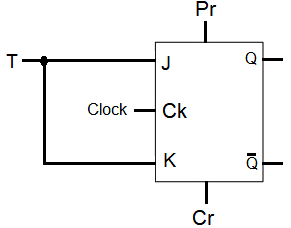
Figure 9. A T flip-flop.
Figure 10 shows the logic symbol for the T flip-flop.
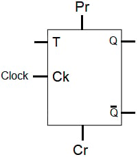
Figure 10. The logic symbol for a T flip-flop.
Commercial CMOS JK FLIP-FLOPS
As an illustration of commercial JK flip-flops, Figure 11 shows a logic diagram of a Fairchild CD4027BC (CMOS Dual J-K Master/Slave Flip-Flop with Set and Reset).
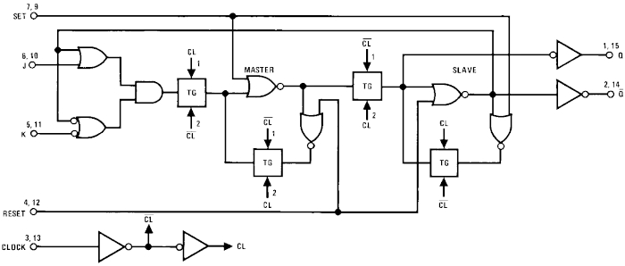
Figure 11. Logic diagram of Fairchild CD4027BC.
According to Fairchild's Datasheet, "The CD4027BC Dual J-K flip-flops are monolithic complementary MOS (CMOS) integrated circuits constructed with N- and P-channel enhancement mode transistors. Each flip-flop has independent J, K, set, reset, and clock inputs and buffered Q and Q̅ outputs."
About CMOS JK, D, and T-type Flip-Flops
A JK flip-flop performs similarly as an SR flip-flop except for the prohibited combination S = R = logic 1 – A JK flip-flop allows both inputs to be logic 1, which makes the flip-flop output toggle with each clock pulse.
The Master-Slave flip-flop eliminates the race-around difficulty. This type of flip-flop combines two JK flip-flops in a cascade configuration. One JK flip-flop is the master, and the other is the slave. This circuit also includes an inverter.
The D-type flip-flop can be used to introduce delay to the data path.
T-type flip-flops have a single data input and act as toggle switches, changing states with each clock pulse.
Flip-flops are available in the digital CMOS IC family.