Facebook
 Google
 GitHub
 Linkedin
Testing Cascode Gallium Nitride FETs
One popular GaN device type is the Cascode GaN FET, which provides even more difficult challenges with its oscillation-prone device behavior. In this article, we specifically discuss how we overcome the challenges associated with Cascode GaN FET measurements.
As we’ve discussed in a previous article, dynamic characterization of Gallium Nitride (GaN) power semiconductor field-effect transistors (FET) present very difficult challenges because of their higher frequency operation and multiple variations of the technology. One of the popular GaN device types is Cascode GaN FET, which provides even more difficult challenges with its oscillation-prone device behavior. In this article, we specifically discuss how we overcome the challenges associated with Cascode GaN FET measurements.
Challenges for Cascode GaN FET Dynamic Testing
Cascode GaN FET came into the marketplace earlier than the other types of GaN power devices because it can provide normally-OFF operation and has a wider gate drive voltage range. However, circuit designers found the device is not so easy to use in an actual circuit, because it is prone to oscillate and its device characterization is very difficult to measure and get repeatable extractions. Many designers must slow down the device operation with a large gate resistor when using it in their circuit, which reduces the benefit of using a fast-speed GaN power device.
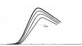
Figure 1 shows divergent oscillation at turn-off. Figure 2 shows a large gate voltage ringing at turn on. Both are related to the unique structure of the Cascode GaN device (cascode of a low voltage Si MOSFET and a high voltage GaN HEMT) shown in Figure 3.

Figure 1: Oscillation at turn off can destroy device and peripheral circuit.

Figure 2: Large oscillation at turn ON.

Figure 3: Cascode structure for high voltage depletion-mode GaN device.
The divergent oscillation seen in Figure 1 is caused by the avalanche breakdown of the low voltage Si MOSFET in the structure. [1] The oscillation of Vgs seen in Figure 2 is related to Vgs unbalance due to the inductance between the MOSFET source and the GaN HEMT gate. The Cascode GaN FET dynamic characteristic measurements are important for both device manufacturers and device users (i.e. power circuit designers), because it is hard to use the device without knowing the condition to avoid oscillation.
Key Considerations When Evaluating Cascode GaN Devices
There are three important components to avoid oscillation when using Cascode GaN devices. One is a snubber circuit, the second is a ferrite bead and the third is the gate resistor (Rg) dependency. The RC snubber circuit consists of a resistor and a capacitor connected in series (i.e. a simple low pass filter). If it is attached between the drain and the source of the power FET, it can reduce or eliminate the sharp voltage rise when the FET turns off. It is important to use the RC snubber circuit to avoid oscillation. It is also important to find the right combination of resistor and capacitor by performing the double pulse test as it will be used in the actual application.
The Ferrite bead reflects and dampens high-frequency noise with its inductive behavior. If an appropriately sized ferrite bead is used, based on the noise frequency on Vgs during the double pulse test, the noise is cleanly removed. There is a chip type ferrite bead that has a spiral structure in the horizontal direction which minimizes stray capacitance and therefore, works effectively to suppress oscillation. Application notes published from Cascode GaN FET manufacturers recommend and describe the use of ferrite beads.
Another key characteristic to evaluate is the Rg dependency. Rg limits the current flowing into gate and therefore, controls the ramp speed of Vgs. The dependency is important when designing power circuits. However, exchanging Rg is not convenient, because the gate resistor for GaN power circuits is usually a SMD type to minimize stray inductance. Therefore, Rg should be soldered and unsoldered to measure the gate resistor dependency.
For Cascode GaN devices, additional capabilities are provided to make its characterization easy and effective.
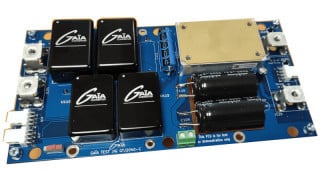
The customized test board for Cascode GaN FET is shown in Figure 4. The test board has ferrite bead terminals and a solderless contact for RC snubbers. An appropriate ferrite bead which suppresses high-frequency energy is selected. For the RC snubber, you can attach or detach it using a through-hole type connector on the board. You can find best RC snubber by measuring characteristics with various combinations. Figure 6 shows measurement results on a Cascode GaN FET with this board. The RC snubber used was a combination of a 15 Ohm resistor and a 33pF capacitor.

Figure 4: Test board for TO-220 Cascode GaN FET.
A solderless replaceable gate resistor mechanism is also implemented. The same board and the same DUT can be evaluated easily using different gate resistors. Figure 7 shows example results using the solderless replaceable gate resistor mechanism. The board shown in Figure 5 is for a TO-220 package device. If the DUT is a SMD package, a board tailored for the SMD Cascode GaN device can be made with solderless DUT contact technology.
The board is plugged into the PD1500A test fixture and is controlled using the PD1500A software user interface.

Figure 5: Solderless DUT contact & replaceable gate resistor.

Figure 6: Test results for Cascode GaN FET (TPH3212PS) Rg=15Ohm

Figure 7: Test results with replaceable gate resistors (500 Ohm & 20 Ohm)
Cascode GaN FET dynamic characterization is challenging due to oscillation-prone device structure. Finding a good operation condition is important for circuit design to take advantage of its superior performance. The PD1500A Dynamic Power Device Analyzer/Double Pulse Tester provides convenient ways to accurately characterize Cascode GaN FETs, using a customized test board to simulate operating conditions with the required peripheral circuitry. For more information, please follow this link or contact your local Keysight representative. https://www.keysight.com/find/pd1500a
About the Authors
Ryo Takeda works as a Solution Architect at Keysight Technologies Incorporated, a company driven to deliver breakthrough solutions and trusted insight in electronic design, test, manufacture, and optimization to help customers accelerate the innovations that connect and secure the world.
Takamasa Arai worked at Keysight Technologies
Bernhard Holzinger works as a Technical Architect at Keysight Technologies Incorporated, a company driven to deliver breakthrough solutions and trusted insight in electronic design, test, manufacture, and optimization to help customers accelerate the innovations that connect and secure the world.
Michael Zimmermann is an R&D Engineer at Keysight Technologies Deutschland GmbH.
Mike Hawes is the automotive and energy solutions planning manager at Keysight Technologies. Hawes holds a Master's Degree in Biomedical Engineering from Colorado State University. He also holds a Bachelor's Degree in Electrical Engineering from Washington State University.
References
1. Avoiding Divergent Oscillation of a Cascode GaN Device Under High-Current Turn-Off Condition, X. Huang, et. al, IEEE Trans. Power Electronics, Vol.32, January 2017.
This article originally appeared in Bodo’s Power Systems magazine.
Related Content