Facebook
 Google
 GitHub
 Linkedin
Active Rectifier Controller with Ultrafast Transient Response and Low Power Dissipation
This article highlights Analog Devices, Inc. LT8672 gate driver that controls the external MOSFET and provides rectification and reverse input protection.
Automotive standards, such as ISO 16750 or LV124, specify that automotive electronic control units (ECUs) may face a supply with a superimposed ac ripple of up to 6 V p-p at up to 30 kH.
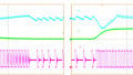
Fast Response for Input Ripple Rectification
Devices such as the LT8672’s gate driver, which controls the external MOSFET, is strong enough to handle ripple frequencies of up to 100 kHz, which minimizes reverse current. An example of such an ac ripple rectification is shown in Figure 1.

Figure 1: Rectification of input ripple.
Low Power Dissipation Compared with a Schottky Diode
The performance of the LT8672 (using the IPD100N06S4-03 as an external MOSFET) can be compared to a Schottky diode (CSHD10-45L) with the setup shown in Figure 2. Here, a 12 V power supply at the input emulates the automotive voltage supply, and the output is loaded with a constant current of 10 A. Thermal performance for both solutions at steady state is shown in Figure 3. Without cooling, the thermal performance of the LT8672 solution is far superior, reaching a peak temperature of only 36°C, while the Schottky diode solution reaches a much higher 95.1°C.

Figure 2: System configuration for thermal performance comparison.
Extra Low Input Voltage Operation Capability
Automotive mission critical circuitry must be able to operate during cold crank conditions, when the car battery voltage can collapse to 3.2 V. With this in mind, many automotive grade electronics are designed to operate down to 3 V input. A Schottky diode’s variable forward voltage drop can present a problem during cold crank, where


Figure 3: Thermal performance comparison: (a) The LT8672 controlled system tops out at a cool 36°C, (b) while the Schottky diode system reaches 95.1°C, causing significant heating over the entire board.
this drop produces a downstream voltage of 2.5 V to 3 V, which is too low for some systems to operate. In contrast, an LT8672 solution guarantees the required 3 V due to its regulated 20 mV voltage drop, which allows for easier circuit design and improved system robustness. Figure 4 shows a comparative cold crank test setup using an LT8650S step-down converter as the downstream test system. The LT8650S output is set to 1.8 V at a constant load of 4 A, and its minimum input operating requirement is 3 V. The results are shown in Figure 5.

Figure 4: System configuration for cold crank test.
When VBATT drops to 3.2 V, the LT8672 controlled system (a) maintains VIN > 3 V, allowing the LT8650S to keep its output VSYS stable at 1.8 V, while in the Schottky diode system (b), the input voltage VIN of the LT8650S drops below its minimum operating voltage, preventing it from maintaining 1.8 V at its output, VSYS.


Figure 5: A system voltage comparison under cold crank (a) using the LT8672 where VSYS stays stable at 1.8 V and (b) using a Schottky Diode where VSYS drops below the minimum operating voltage.
Integrated Boost Regulator
Many alternative active rectifier controllers use a charge pump to power the gate driver. These solutions often cannot provide strong gate charging current and a regulated output voltage, which limits the frequency range and performance of continuous rectification. The LT8672’s integrated boost regulator provides a tightly regulated gate driver voltage with a strong gate driver current.
Conclusion
The LT8672 active rectifier controller is able to rectify high frequency ac ripple on automotive supplies. It uses an integrated boost regulator to drive a MOSFET for ultrafast response during continuous rectification, which is an improvement over charge pump solutions. It provides rectification and reverse input protection with low power dissipation and an ultrawide operational range (desirable for cold crank) in a tiny 10-lead MSOP package. In addition, the LT8672’s active protection has a number of advantages over Schottky diode designs, such as minimal power dissipation and a small, predictable, regulated 20 mV voltage drop. The LT8672 also includes features to satisfy supply rail requirements in automotive environments:
- Reverse input protection to –40 V
- Wide input operation range: 3 V to 42 V
- An ultrafast transient response
- It rectifies 6 V p-p up to 50 kHz and it rectifies 2 V p-p up to 100 kHz
- Integrated boost regulator for the FET driver outperforms charge pump devices
Figure 6 shows a complete protection solution.

Figure 6: LT8672 active rectification/reverse protection solution.
About the Author
Bin Wu was born in Zhejiang, China, in 1985. He received his Ph.D. in electrical engineering from the University of California, Irvine, CA, in April 2016. From April 2016 to July 2017, he was a post-doctoral research associate at the University of Maryland, College Park. After that, he worked at Maxim Integrated. Since November 2017, he has been an application engineer with Analog Devices, San Jose.
His interests include electrical vehicle power architecture, high power density step-up/step-down dc-to-dc converters, switched capacitor converters, modeling, and renewable energy integration systems. He can be reached at Bin Wu Analog Email Address.
This article originally appeared in the Bodo’s Power Systems magazine.
Related Content