Facebook
 Google
 GitHub
 Linkedin
A New Dual-in-Line Surface Mountable IPM for Motor Drive Applications
This article features Alpha and Omega Semiconductor dual-in-line SMD-type intelligent power module (IPM) specialized for low-power BLDC motor-drive systems.
This article introduces a new dual-in-line surface-mount device (SMD)-type intelligent power module (IPM) specialized for low-power BLDC motor-drive systems such as fan motors used in home appliances air-conditioners that require highly compact size with reliable and efficient design allowance. The proposed ultra-compact surface mountable IPM has an 18mm x 7.5mm package dimension and is composed of three-phase MOSFET bridge and gate control ICs. The integrated functions include bootstrap circuit, under-voltage lockout (UVLO) protection, temperature monitoring (VOT) and over-temperature protection. It can greatly help to simplify the inverter design in conjunction with smaller footprint PCB and enhance the reliability and cost reduction of the system. The key features associated with design and application consideration are described.
Introduction
A BLDC-based inverter system is widely used in such consumer applications as refrigerators, washers, dryers, room air-conditioners, and fan motors because it is quicker, quieter, and more energy efficient than the conventional solutions using dc motors or ac induction motors with on/off control. Nowadays, its demand and expansion is becoming mandatory requirement due to energy saving and regulations. The key technology that has enabled this progress is an inverter technology, particularly the transfer mold integrated power module.
Since 1998 transfer-molded package technology has been successfully applied to IPMs for motor-drives utilizing IGBTs, freewheeling FRDs and MOSFETs as power switches, and high voltage integrated circuits (HVICs) as the gate driver [1]-[6]. The voltage and current ranges of the IPM have been successively increased up to 1200V and over 50A. The advantages of transfer mold technology are mainly dual use of the copper lead-frame as electrical conductor that can dramatically reduce the package size as well as the manufacturing cost.
The low-power BLDC-fan motor inverter design used in air-condition-ing and purifying systems for home appliances has highly strict cost and size limitation requirements due to its huge quantity and limited product space. There have been several development efforts on one-chip inverter solution for this application by integrating the lateral IGBTs with control circuit on a single silicon chip. They can provide further smaller circuit area, however there are several drawbacks. There is no flexibility of circuit design, and moreover, the power dissipation is concentrated in one location, which can cause a problem of thermal management. The switching performance and ruggedness of LIGBT are less than that of the conventional switching device, which result in very limited application range and controllability.
For these small fan motor-drive applications, Alpha and Omega Semiconductor has developed a new surface mountable IPM. The proposed module consists of advanced MOSFETs and gate driving ICs in a new package, as highly compact, reliable and cost-effective solution. The IPM has extremely small package size thanks to partial super-junction MOSFET technology, HVICs with integrated boot-strap circuit, and optimized design of the package, so that one can significantly enhance the cost-effective development of the system reducing the inverter board size and obtaining easy and reliable PCB assembly.


Figure 1: Proposed IPM. (a) External view, (b) Internal equivalent circuit and pin configuration
Compact Package and Electrical Design
Figure 1(a) shows the outline of the 19-pin counting package of the proposed dual-in-line IPM. A lead-frame construction has been employed and multi chips of MOSFETs and gate-drive ICs have been soldered on it. The total surface required from this package is 18mm x 10.3mm = 185.4mm2 including pin leads. A discrete solution utilizing three pieces of SO-8 packaged HVIC half bridge driver each having a surface demand of 5mm x 6.2mm = 31mm2 and six pieces of DPAK packaged power devices each having a surface demand of 6.5mm x 10mm = 65mm2 requires 483mm2(= 3x 31mm2 + 6 x 65mm2) of the surface. Thus, the conservatively summarized size advantage, ignoring the space for the complicated routing, can be a PCB space requirement of only 38% compared to that of a discrete solution. Figure 1(b) illustrates the internal equivalent circuit and pin configuration which is composed of six MOSFETs as power switching devices, high side gate-driving HVIC including integrated bootstrap components, and low side gate-driving LVIC including temperature sensing (VOT) and fixed over-temperature protection function. Signal COM is located with the power ground N terminal. There are two u-phase output pins U1 and U2 which need to be connected by external PCB wiring.

Figure 2: Vertical structure of a new MOSFET
Figure 2 indicates the vertical structure of a new MOSFET that is integrated in the IPM. It has been newly developed for motor drive applications which has partial super-junction configuration. The power density Rds·A has been improved by over 30% compared to conventional planar MOSFETs, and it can provide more suitable EMI controllability than super-junction devices.

Figure 3: Turn-ON switching behavior

Figure 4: Short-circuit ruggedness
An appropriate turn-ON switching performance has been achieved by the micro fabrication and wafer process technology for the designed partial super-junction MOSFET. From the experimental waveforms shown in Figure 3, we can clearly state that Irr, Qrr and trr performances are comparable to those of the conventional planar MOSFET technology used in 3-phase motor-drive applications concerning EMI, noise and power dissipation.The optimal selection and design of the gate resistors, Qg, and Vth have been made to prevent the shoot-through issues at turn-ON.
Figure 4 shows the evaluation waveforms of short-circuit ruggedness of the MOSFET. It shows over 100us withstanding time that can be good enough for the stable design and control of the inverter.
The switching operating SOA has been evaluated in the light of the practical IPM inverter circuit condition including parasitic circuit inductances. We have increased the applied dc-link voltage up to over 600V although the proposed IPM has 500V of voltage rating limited by the MOSFET breakdown voltage (BV). To guarantee 500V, the typical BV design of the MOSFET is based on 550V. It is noted that there is no any abnormal phenomenon in the switching operation with the condition of 550V of dc-link voltage due to highly rugged MOSFET design as is shown in the waveforms of Figure 5. When we apply over 600V of dc-link voltage, it is observed that abnormal turn-ON currents occur because of partial shoot-through current. But there was no destruction failures of the IPM due to strong short-circuit ruggedness.

Figure 5: Switching SOA test
High precision temperature converting circuit has been integrated into the embedded gate-driving LVIC by the laser-trimming technology. VOT pin generates analog output voltage signal that is corresponding to LVIC temperature. It is possible to use the IPM at a junction temperature much closer to the tolerable maximum rating. Figure 6 illustrates the output characteristics of VOT. Different lot samples have been evaluated to verify the tolerance of VOT performance at the real application condition. It is significant to observe that the LVIC

Figure 6: LVIC temperature output of the proposed IPM
temperature is accurately measured through the appropriate design of the LVIC and its precise waferprocess technology. Due to the tiny package size of the proposed IPM, the voltage output of VOT will make fast response time according to the junction temperature of the MOSFET. It can provide simple, cheap and accurate solution for the application.

Figure 7: Operating thermal simulation at fSW=20kHz, PF=0.8, VDC=300V, VCC=15V
Application Consideration
Thermal simulation has been carried out considering 50W-BLDC motor operating condition. The 20kHz of PWM switching frequency has been applied that is considered as normal frequency in the field to avoid audible noise. From the simulation result shown in Figure 7, it is observed that FET 4 has the highest junction temperature and low side FET 1 has the lowest temperature rise. The temperature difference was 8°C between the two MOSFET chips. It can be mentioned that the power rating of the module would be limited by the center chips of FET 3 and FET 4. The LVIC temperature shows 17°C lower than FET 4 one under the applied operating condition.
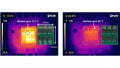
Figure 8 explains the simulation summary about the application example of the proposed IPM, where the simulation has been carried out based on the continuously operating power condition. In Figure 8(a), the power loss was calculated at 150°C of junction temperature. It was assumed that the maximum operating junction temperature of FET 4 determines the maximum power rating. It should be noted that allowable operating power is decided and controlled by the case temperature Tc as shown in Figure 8(b). The temperature difference between LVIC and FET 4 can reach over 30°C depending on operating power, as depicted in Figure 8(c). In the module design, the fixed OT protection level is typ.130°C of the LVIC temperature. Figure 8(d) indicates FET 4 temperature is slightly higher than FET 3.Figure 9 illustrates an application circuit example and experimental set up. The internally fixed over-temperature protection function can be disabled by connecting 10kΩ of pull-down resistor to VOT (pin number 11) or enabled by no connection of the resistor. The analog voltage output VOT to detect the LVIC temperature is always activated no matter what the pull-down resistor connection. It is recommended to use R2-C5 (2kΩ-10nF) filter to avoid noise malfunction for temperature sensing function.Figure 10 shows the temperature profile taken by an infrared camera. It is shown that the temperature of the center area of MOSFET chips is about 14°C higher than that of the LVIC part at 50W inverter operation.


Figure 8: Simulation result. (a) Power loss, (b) Allowable operating current, (c) Temperature rising, (d) Temperature difference
Figure 11(a) shows the experimental result for Enabled OT protection function. The OTP is activated when the LVIC temperature reaches its trip level, typ. 130°C. At that point, the measured case temperature Tc was 144°C. The OTP operation is deactivated when the LVIC temperature decreases to its reset level, typ. 100°C. It is obvious that 30°C of the OTP hysteresis level has been accurately designed.
The temperature rise in the case of Disabled OT protection has also been tested by connecting 10kΩ of pull-down resistor to pin 11 as is shown in the measurements of Figure 11(b). It is observed that the LVIC temperature reaches 144°C when the case temperature Tc becomes 160°C. The inverter system has been shut down intentionally for safety.
Another interesting investigation of the IPM application is in the variation of the bootstrap capacitor voltage, as shown in Figure 12. The inverter output frequency was running at 60Hz with 20kHz of switching frequency. The bootstrap voltage is depicted with the output current

Figure 9: Application circuit example

Figure 10: Temperature profile by an infrared camera
of the inverter. When the current was positive, the bootstrap voltage VBS increases close to VCC=15V, but it dropped to almost 13V when CBS=1uF. This is caused by different charging mechanism according to the current direction. When the output current is positive, it flows through either a high-side MOSFET or a low-side body diode. In this case, the bootstrap capacitor CBS is charged when the low-side body diode is turned on. The charging peak voltage will be slightly lower than VCC supply in the MOSFET IPM if the body diode voltage VSD is not higher than the forward voltage drop of bootstrap diode during that charging mode. When the output current is negative, the charging voltage will drop as much as the forward drop of MOSFET when the low-side MOSFET serves as the active switching device. However, the bootstrap voltage is the gate driving power supply of the high-side MOSFET and critical only when the current is positive. When the current is positive, the bootstrap voltage does not vary much due to the low VSD of MOSFET, eliminating the need of large bootstrap capacitor. One can have small bootstrap capacitor that is enough to hold the bootstrap voltage against the standby current of HVIC, only when the output current is positive. In the proposed IPM, the high-side UVLO is designed to be typ. 10V.
Conclusion
We have presented the new ultra-compact surface mountable IPM for low-power BLDC fan motor-drive system used in home appliances, where ruggedness, temperature protection, power dissipation, electromagnetic interference, noise immunity, and cost reduction are primary concerns. Although the small MOSFET-IPM has reached certain maturity, there are still some issues to address to further increase its performance and reduce its cost. Moreover, advances in enabling IPM technologies and their applications continuously open new development trends and industrial interest. It is expected that the proposed IPM can significantly enhance easy and reliable design of the inverter board, and can allow considerable cost-effective solution of the system.

Figure 11: Over-temperature operation. (a) Enabled OT, (b) Disabled OT

Figure 12: Variation of the bootstrap capacitor voltage
References
- S. Shirakawa, T. Iwagami, H. Kawafuji, M Seo, and K. Satoh, “A New Version Transfer Mold-Type IPMs with Compact Package,” PCIM-Asia 2005.
- T. Iwagami, K. Satoh, K Shomei, H. Kawafuji, S. Shirakawa, and T. Tanaka, “ A Development of 30A/600V Super mini DIPIPM,” IPEMC 2006.
- Yuji Ishimatsu, Motohiro Ando, NobuhiroHase, and KazuhideIno, “High Efficient Super Junction MOSFET Intelligent Power Module,” PCIM 2015.
- Sungun Shim, Taehyun Kim, Minsub Lee, Junbae Lee, and Daewoong Chung, “A New Low Loss MOSFET Intelligent Power Module for the Low Power Motor Drive Applications,” PCIM 2014.
- Carmelo Parisi, Gaetano Belverde, and AlessioCorsaro, “STMicroelectronics Super-Junction and Ultrafast MOSFET vs IGBT Technologies in Low Power Motor Drives,” PCIM 2017
- Yazhe Wang andMaki Hasegawa, “New Transfer Mold SMD type IPM with integrated RC-IGBT, Bootstrap Diode and Capacitor,” PCIM 2018.
This article originally appeared in the Bodo’s Power Systems magazine.