Facebook
 Google
 GitHub
 Linkedin
A Novel Circuit Topology for Turning a ‘Normally On’ GaN Transistor into ‘Normally Off’
This article discusses how D-mode GaN transistors make themselves excellent building blocks for the next generation power conversion systems.
In the past year, it has become clear that Gallium Nitride (GaN) power transistors have been successfully launched in end user’s products, as has been reported by the various GaN device manufacturers. Examples include Transphorm products in Corsair’s AX1600i Power Supply Unit (PSU) and Bel Power Solution’s TET3000-12-069RA power supply, and Infineon products in Eltek’s Flatpack2 SHE power conversion module. The system performance and cost benefits in, for instance, a Totem Pole Power Factor Correction (PFC) in high-end AC/DC power supplies (such as is the case in the Corsair and Bel Power Solutions’ products) are so significant that GaN transistors are clearly destined to replace the incumbent Si MOSFET transistors. Increased volume will lead to reduced GaN transistor pricing and in turn to accelerated adoption in PFC, DC/DC and inverter applications.
Si MOSFETs have been improved for decades but have started to reach physical limitations in terms of density and efficiency, preventing additional significant improvements. The increase in input and output capacitance as Rds(on) is reduced, hampers high switching frequency operation due to the increase in switching losses. GaN transistors on the other hand, which are characterized by significant lower capacitances, are only at the beginning of a long road of improvements and breakthroughs, made possible with the superior material and physical properties such as high conductivity, high energy gap and high electric field – as compared to Si.
There are two major versions of GaN-on-Si power transistors, Enhancement mode (E-mode) and Depletion mode (D-mode) transistors. In their natural state, an E-mode transistor is a ‘normally off’ (device is ‘off’ at Vgs=0V) and requires a positive Vgs to turn ‘on’. A D-mode transistor is ‘normally on’ (device is ON at Vgs=0V) and requires a negative Vgs to turn ‘off’.
E-mode GaN transistors available in the market today all make use of gate doping to increase the threshold voltage and to improve dynamic Rds(on). It remains a challenge to find the optimal trade-off between performance (such as Vth drift) and reliability (lifetime) with high voltage E-mode technology. On the other hand, the lack of doping makes D-mode devices inherently more robust and reliable compared to E-mode devices. The doping activation efficiency in GaN is only 12-20%. In addition, for every dopant there are 5 to 7 crystal defects created. As a result, undoped GaN has 2 to 3 orders of magnitude less crystal defects than doped GaN. High voltage D-mode devices are therefore a better fit to qualify for the stringent standards such as the automotive AEC-Q101.
D-mode transistors have been turned into Normally ‘off’ devices using a cascode topology, or in the case of VisIC with a proprietary ‘normally off’ (NOFF) circuit and driving scheme. This will be explained in more detail further down in this article.
When GaN is grown naturally on a Silicon substrate, the resulting device layers and structure are that of a D-mode GaN transistor, as shown in Figure 1.
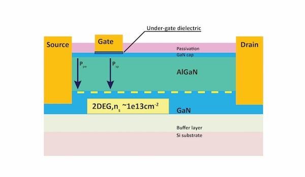
Figure 1a. VisIC D-mode GaN Transistor Structure
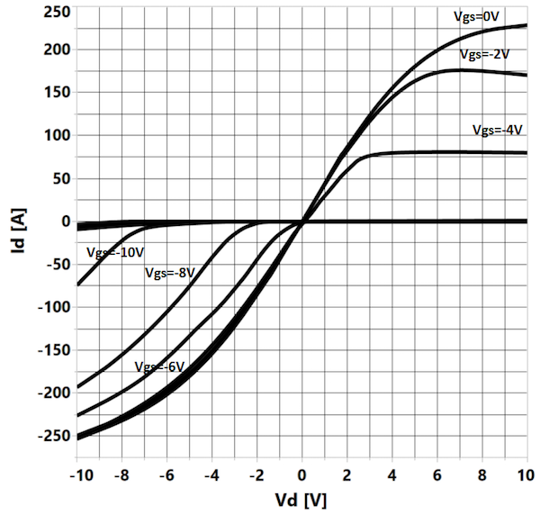
Figure 1b. Native I=f(Vgs) characteristics (b).
VisIC’s GaN transistor assemblies have a maximum gate drive of 15V and a gate voltage threshold or noise immunity of 5V (typ), making them easy to use and robust. The combination of its low switching energy and excellent thermal performance, makes it possible to get more power out of the V22N65A (22mOhm typ) devices than any other GaN device on the market. Furthermore, since the VisIC GaN devices do not include a body or attached diode, they are void of the reverse recovery problems and hence offer additional design flexibility.
The VisIC ‘Normally Off’ Configuration and Level Shifting
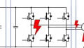
The drive voltage shifter or reversal circuit and build-in ‘normally off’ state circuit around the GaN transistor Q1 (Fig. 2) has three functions: to assure ‘normally off’ operation, to shift or reverse the gate drive voltage signal such that a conventional (0V - 15V) driver can be used, and to enable operation with one power supply. The latter provides considerable savings especially when the transistor is used on the high side. Fig. 2 shows the GaN MCM (Multi-Chip Module) driven by a common MOSFET gate driver which is powered by a single power supply Vdd.
'Normally Off’ Configuration
The ‘normally off’ configuration is implemented by Q2, Q3 and associated passive elements. Without a Vdd power supply, the assembly is not conducting because the series, P channel MOSFET transistor Q2, is ‘off’ due to the fact that its gate to source voltage is zero. This transistor is a low voltage MOSFET, chosen to have a very low Rds(on) when conducting - in the order of 1mΩ. This adds little to the total resistance of the GaN assembly (between 22 mΩ and 80 mΩ depending on the model) when the module is ‘on’.
Once the auxiliary supply starts to rise, the Vdd line is clamped to the source of Q1 by virtue of the body diode of Q3. Nothing happens until Vdd reaches the breakdown voltage of the Zener diode D2. This turns on Q4 which, in turn, pulls down the voltage of R to the AuxGnd potential. This potential is negative with respect to the sources of Q1, Q3 and Q4 by virtue of the fact that the source of Q1 is at Vdd potential (initially via the body diode of Q3). Once the voltage of the gate’s resistor R1 becomes negative with respect to the sources of Q3 and Q2, these P channel MOSFETS turn ‘on’ - putting the assembly into the ‘ready’ state.
Voltage Level Shifter
As pointed out above, once the assembly is in the ready position, the Vdd line is connected to the source of the GaN MOSFET Q1 and therefore the Gnd potential is negative with respect to the source of the GaN. This assures an ‘off’ state of the GaN when the output of the driver is low with respect to its supply. When the output of the driver is high, the gate of the GaN is effectively shorted by the high side of the driver as shown by the dashed red line in Figure 2.
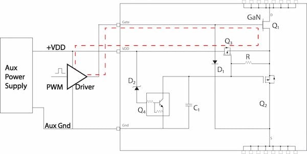
Figure 2. The VisIC V22N65A and typical drive arrangement. The broken red line is the path of gate ‘turn on’ current while the dotted blue line is the ‘turn off’ gate current path.
Diode D1 protects the system against harmful overvoltage due to gate path inductance as well as against noise coupling via the gate-to-drain capacitance of the GaN. Another pivotal function of diode D1 is the protection of the GaN transistor in the absence of Vdd, if power is turned and thus a high voltage is imposed on the GaN’s drain. In this case, without the diode, the static gate potential may cause the GaN to conduct which, in turn will subject the low voltage Si MOSFET Q2, to a high voltage which will cause a breakdown of the device. This is remedied by D1 which clamps the gate of the GaN to Gnd. If, upon the onset of a high voltage on the drain of the GaN it will partially conduct, the source will become positive with respect to the gate until the threshold, Vth, is reached and the GaN will shut down. Hence the maximum voltage on Q2 in the off state is about Vth.
When the output of the driver goes ‘low’ again, the driver feeds a negative current to the gate of the GaN, as shown by the dotted blue line. This clamps the gate to the Gnd potential which is negative with respect to the source of the GaN.
Performance
Typical performance of the GaN assembly (VisIC V22N65A) is depicted in Fig 3a. The unit was loaded by a 15Ω resistor connected to a voltage source of 400V and hence the current was 28A. The unit was driven by a Si82394AD-IS driver. The fall time of the driver signal was measured to be about 12ns and the rise time of VDS was 6.4ns Figure 3a).
The current switching details of the GaN transistor at ‘turn on’ and ‘turn off’ are shown in Fig. 3b. The rise time of the drive signal, in this case, is about 10ns. The current starts to rise as soon as Vgs hits the threshold voltage. The somewhat exponential shape of the turn on current is due to the stray inductance of the circuit which is calculated to be approximately 800nH. This stray inductance causes the disturbance at the ‘turn off’ of the transistor seen also in Figure 3a.
It should be noted that while the driver signals are in the 0-12V range, the voltage reversal circuit of the VisIC V22N65A will deliver a -12V to 0V to the gate of the GaN.
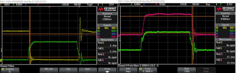
Figure 3: Experimental measurements of the GaN (VisIC V22N65A). Left: Driver signal (Green) and VDS (yellow) at current ‘turn off’. Right: Driver signal (Green) and ID (red) of GaN at current ‘turn on’.
Conclusions
The improved material, as well as physical and electrical characteristics of the D-mode GaN transistors, makes them excellent building blocks for the next generation power conversion systems that need to address stringent requirements of efficiency and size without compromising reliability. Although the native D-mode GaN is a ‘normally on’ device, the VisIC GaN devices, such as the V22N65A, are ‘normally off’ assemblies that are directly compatible with common, 0 to 15V MOSFET gate drivers powered by a single power supply. This transparency is made possible by a ‘normally off’ circuitry and a drive level shifter discussed in this article.
About the Authors
Shmuel (Sam) Ben-Yaakov received the BSc degree in Electrical Engineering from the Technion, Haifa Israel, in 1961 and the MS and Ph.D. degrees in Engineering from the UCLA, in 1967 and 1970 respectively. He is a Professor Emeritus of the Department of Electrical and Computer Engineering, Ben-Gurion University of the Negev, Beer-Sheva, Israel. He published more than 300 papers and was granted more than 30 patents and specializes in Power Electronics, Analog Electronics Circuits.
Luc Van De Perre holds an MBA at Santa Clara University and a Master's and Bachelor's Degree in Electrical Engineering at KU Leuven and KIHK, Belgium respectively. he has solid business and technical skills in power electronics as well as strong knowledge of the technical requirements in different power applications such as hybrid and electric vehicles, networking & communications equipment, servers, industrial equipment, motor drives, UPS systems, charging stations, PV and LED lighting. He worked at VisIC Technologies.
This article originally appeared in the Bodo’s Power Systems magazine.