Facebook
 Google
 GitHub
 Linkedin
UniversityWafer Looks to Implement Semiconductor Production in Low Earth Orbit
Silicon wafer manufacturer UniversityWafer has announced plans to build a system capable of producing power wideband semiconductor materials in low earth orbit.
The system will reportedly work through Chemical Vapour Deposition (CVD), with a range of growth temperatures up to 800C and continuous growth time up to six months.
According to the company, the focus of the new project will not be on R&D, but on designing scalable components that need to be manufactured in orbit, starting with semiconductor wafers.
UniversityWafer
The company provides researchers with wafers of different dimensions and materials to support research in the field.
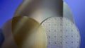
In particular, UniversityWafer deals with silicon carbide (SiC) wafers and other semiconductor substrates and services, including thermal oxide, nitride, thin films, and dicing.
The Boston-based company has in the past provided various research institutions with glass, sapphire, silicon, III-V, and II-VI wafers for the manufacturing of a variety of innovative components, including PN Junctions and solar cells.
Noticeably, a team of researchers from Stanford University has recently used UniversityWafers’ 100mm Silicon Item #783 to fabricate photonic structures capable of controlling solar absorption and thermal emissions.
The findings of the study hold considerable potential for the development of more power-efficient solar panels and electric vehicles.
Building on its manufacturing expertise of wafer technologies, the company has now announced the creation of a new system designed to manufacture power wideband semiconductor materials such as gallium nitride (GaN) and SiC in low earth orbit.
Exploring ‘Space-based Wafer Fabrication
Commenting on the news, UniversityWafer founder Christian Baker clarified the space platform will be capable of Chemical Vapor Deposition as it orbits around the earth.
“No gravity is promised to enhance wafer purity and crystals,” he explained.
According to the executive, the company is aware of the similar experiments performed on Spacelab and the Wake Shield Facility, but also highlights the differences with the upcoming UniversityWafer project.
“For conventional silicon wafer production, we would agree there is little demonstrated advantage, both in terms of quality and relative cost,” Baker said.
However, the executive added he believes the development of compounds and other exotic semiconductors offers a demonstrated advantage for free flyers.
“UniversityWafer’s partners will use a dedicated facility just for crystal growth, not attached to the International Space Station (ISS) or any other vehicle, both in terms of reduced convection and ambient contamination,” Baker explained.
The project will not focus on research and development efforts, however, but on individuating components that can be efficiently manufactured in orbit, and then scaled through multiple missions per month.
“UniversityWafer, with our partners, are working on providing researchers with a vehicle that allows not only testing theories but actual production in the low orbit of space,” reads a page on the company’s website.