Facebook
 Google
 GitHub
 Linkedin
Low-Power Printed Electronics Could Use Light and Electromagnetic Waves to Operate
Researchers uncover a new approach for developing more efficient printed electronics that could use light and electromagnetic waves from the surrounding environment to operate.
The 3D printing of electronics may still seem to be something of a budding area of technological development. Despite this, 3D printing electronics has benefited the power electronics industry in a number of ways and is continuing to grow its influence in this sector.
Collaboration between researchers from Soochow University (China) and researchers from the Chinese Academy of Sciences, the University of Cambridge, and Saudi Arabia
has garnered the development of a new approach for printed electronics. The approach allows for low-cost printed devices to be recharged with ambient light or radiofrequency noise.
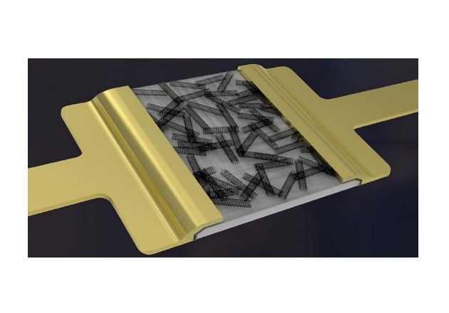
Artist's impression of a hybrid-nanodielectric-based printed-CNT transistor. Image courtesy of Luis Portilla (Soochow University).
While 3D printing methods have been progressing with regard to technique and incorporation of new ink materials to make the printing of electronic devices more cost-effective and more intricate in design, low energy and energy consumption is still a challenge. As the world grows to adopt electronic systems and device networks as part of the internet of things (IoT), manufacturers are looking to create electronic devices that are not only cheap to manufacture, but that also require minimal power to run.
The Research
In their research published in the journal ACS Nano, the researchers detail the development of high-performance transistors which enable digital circuits to run with wide noise margins, ultra-low operating voltages (≤0.5 V), all the while displaying record-low power consumption (≤1 pW/μm).
The design of the thin-film transistors incorporated the use of solution-processed polymer-sorted semiconducting carbon nanotube networks (sc-SWCNTNs). These are essentially ultra-thin cylinders of carbon that act as an ambipolar semiconducting material. An ambipolar transistor belongs to a class of transistors that can transport both positive (holes) and negative (electrons) charge carriers through the semiconducting channel at the same time. This process occurs in a region of operation called ‘deep subthreshold’. This is essentially regarded as a transistor’s OFF-state.
In a recent news release, Luigi Occhipinti, research co-author from the Department of Engineering at Cambridge, provided his take on the findings: “Thanks to deep-subthreshold ambipolar approach, we created printed electronics that meet the power and voltage requirements of real-world applications, and opened up opportunities for remote sensing and ‘place-and-forget’ devices that can operate without batteries for their entire lifetime.”
Occhipinti also commented on the potential benefits of the research for the power electronics community: “Crucially, our ultra-low-power printed electronics are simple and cost-effective to manufacture and overcome long-standing hurdles in the field.”
“Our approach to printed electronics could be scaled up to make inexpensive battery-less devices that could harvest energy from the environment, such as sunlight or omnipresent ambient electromagnetic waves, like those created by our mobile phones and wifi stations,” said co-lead author Professor Vincenzo Pecunia from Soochow University.
Researchers also commented further, saying that the research may be able to pave the way for the development of battery-less devices that can harness energy from our surroundings, which includes light and omnipresent ambient electromagnetic waves that are emitted from wifi stations and mobile phones.
This kind of technology has the potential to power smart homes, a number of consumer wearables, medical devices, and provide infrastructure monitoring for the next generation of IoT ecosystem users and inhabitants.