Facebook
 Google
 GitHub
 Linkedin
Graphene enables Fast-Charging Li-ions with Higher Energy Densities
In the development of advanced lithium-ion batteries, improving one property without sacrificing others is challenging due to the trade-off nature among the key parameters. In a recent paper in Nature Communications, a research team from the Samsung Advanced Institute of Technology reported a chemical vapor deposition process to grow a graphene-silica 3D assembly, called a graphene-ball to provide both fast charging and high volumetric energy densities in Li-ion batteries.
Its hierarchical 3D structure with the SiOx nanoparticle center allows even 1 wt% graphene-ball to be uniformly coated onto a nickel-rich layered cathode (LiNi0.6Co0.1Mn0.3O2) via mild Nobilta milling. The graphene-ball coating improves cycle life and fast charging capability by protecting the electrode surface from detrimental side reactions and providing efficient conductive pathways.
The graphene-ball itself also serves as an anode material with high specific capacity of 716.2 mAh g-1. A full-cell incorporating graphene-balls increases the volumetric energy density by 27.6% compared to a control cell without graphene-balls, showing the possibility of achieving 800 Wh L-1 in a commercial cell setting, along with a high cyclability of 78.6% retention of the initial capacity after 500 cycles at 5C and 60 degrees C.
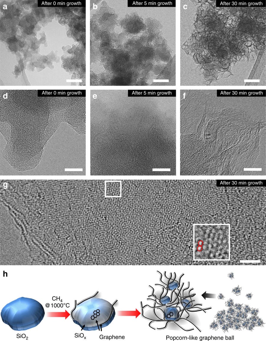 Graphene growth from SiO2 nanoparticles. a–c TEM characterization a before CVD growth, b after 5 min growth, and c after 30 min growth (scale bars, 50 nm). d–f Their respective magnified images (scale bars, 10 nm). g Higher magnification image of graphene after 30 min growth and its atom-level view from the white box (inset) (scale bar, 2 nm). h Graphical illustration of popcorn-like graphene growth from SiO2 nanoparticles
Recent innovations in materials science such as the development of graphene balls for Li-ion batteries have led to a boom in the creation of new devices, allowing for a rapid shift from analog to digital in a relatively short amount of time.
In the past, materials were researched, developed and perfected long before they were applied to devices. Take liquid crystals, for example. They were first discovered in the late 1800s, and for decades were studied and defined in the academic realm. It wasn’t until the 1960s―almost a century later―that they were utilized in commercial products. Similarly, it took 30 years after its invention for lithium metal oxide to even be tested in batteries, and another decade before it made its official commercial market introduction.
Once materials such as these were introduced, however, they allowed for a steady and fairly rapid increase in device performance. In the display industry specifically, there has been enormous growth in the market because of such advancements up until now.
However, as the market becomes increasingly saturated, electronic materials innovations are beginning to fall behind the device revolution. This is mostly due to the fact that the device product life cycle is becoming much faster than that of the material. Now, the device itself is facing the limitations of this revolution in terms of product performance and functionality without the aid of novel materials.
To ensure consistent advancements and optimum functionality, both materials and devices have to be synchronized throughout the development process from the earliest stages of research so that performance requirements can be properly understood.
This was the message of the plenary session led by Dr. Hyuk Chang, Executive Vice President , Samsung Advanced Institute of Technology (SAIT), at the 9th International Conference on Quantum Dots held earlier this month.
Chang noted that the synchronization of materials research and device development can accelerate the enhancement of both the devices and the materials that they are made of, thus revitalizing the market.
“After all, innovation comes in many forms, and source technology is a foundational one,” Chang said.
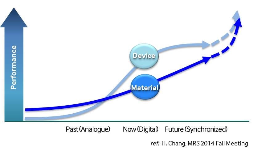 The speeds of material and device innovation have changed over time. SAIT now aims to synchronize the two.
At Samsung, there are numerous organizations that carry out research and development. These include SAIT, where the company pioneers long-term, radical researches with five to ten year or more horizons; the R&D centers that explore next-generation products and platform technologies one to three years in advance; and business unit development teams that focus on commercialization, applying these latest technologies in product development.
Samsung is increasingly synchronizing its R&D efforts to bring core technologies like new materials to products more quickly.
One example is quantum dot technology. Confident that this specific technology could ultimately drive the future of display, among other areas, Samsung has researched the material and its advantages in earnest. In fact, researchers at SAIT started focusing on quantum dot technology over a decade ago, and have since registered numerous patents on the subject.
Through constant testing, evaluating and verifying the material from the earliest stages of device design, Samsung was able to incorporate quantum dots to create a revolutionary line-up of products―its 2015 SUHD TVs.
 Example of a synchronized research roadmap
In doing so, the technology allowed for highly accurate color expression and better, brighter picture quality while improving overall energy efficiency at a lower cost―all with cadmium-free quantum dots. Considering that this was the first commercial application of the material, it created quite a buzz among academics in the field who had been eagerly anticipating such a milestone.
Despite these accomplishments, Samsung wanted to improve upon this technology and did so with its 2016 SUHD TVs, making them even more energy-efficient, and allowing them to display the picture quality more accurately.
“As a materials scientist, my previous work was in small-scale labs,” Chang explained. “It was overwhelming to see this technology make its way to mass production and even hit center stage at the industry’s top events like CES in just a decade. That’s the speed and scale of Samsung.”
As Samsung continues to research and refine the technology, the company predicts that quantum dots will further enhance display devices.
Chang noted that quantum dots could be applied in other ways, too, such as to improve the accuracy of image sensors, which could significantly advance autonomous cars. Experts note that the technology also has great potential in the areas of chemo- and bio-sensing. In fact, researchers at SAIT have already begun to utilize quantum dot technology in these areas, and are eager to continue to progress these developments.
“Just as Samsung’s SUHD TVs were realized by evolutionary quantum dot materials and boundless research for discovering novel physical phenomena, functional materials, value-added materials and next-generation devices must be closely interconnected,” Chang stated.
This, he believes, will accelerate materials innovations, leading to new functionalities in devices and the creation of novel devices. The synchronization of materials research and device development will also help to breathe new life into the massive global materials marketplace. By consistently providing added value with new materials, Samsung hopes to continue to revitalize the electronic devices industry.