Facebook
 Google
 GitHub
 Linkedin
Toshiba Launches New Line-up of MOSFETs and Schottky Diodes for Wireless Power Transfer Applications
Toshiba Electronics Europe (TEE) has expanded its line-up of small-signal, medium-power Schottky barrier diodes (SBDs) and MOSFETs that are especially suitable for wireless power transfer applications. The range of devices covers single and dual n- and p-channel MOSFETs as well as SBDs. The miniature devices are optimised to meet the low power consumption and compact form factor demands of wireless charging applications for portable, battery-powered devices such as mobile phones, digital cameras and video recorders, tablet computers and notebook PCs.
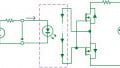
Among the new devices is a MOSFET ideally suited to load switching in a wireless charging transmitter circuit. The 30V SSM6N55NU is the industry's highest performance dual -channel MOSFET in a UDFN6 package measuring just 2.0mm x 2.0mm x 0.75mm. A drain current of just 4A and a maximum ON resistance (RDS(ON)) down to 46mΩ ensure high-efficiency operation. The device joins a comprehensive family of MOSFETs that combine low RDS(ON) with ultra-compact packaging.
Toshiba's latest single and dual SBDs are rated for reverse voltages of 30V and feature very low forward voltage (VF) ratings down to just 0.45V. Ultra-miniature packaging options range from USC (SOD-323) with dimensions of 2.5mm x 1.25mm x 0.9mm to CST2B options that measure just 1.2mm x 0.8mm x 0.6mm.
Applications for the new MOSFETs and diodes include load switching, low-voltage rectification, bridge circuits and reverse current protection.