Infineon Introduces MOSFETS for Static Switching Applications
The new additions to the 600V CooMOS S7 family are aimed at high power, low frequency product designs
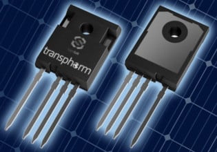
The CoolMOS S7 and the CoolMOS S7A are N-channel devices aimed at industrial and automotive applications, respectively.
Image courtesy of Infineon
What is Static Switching?
Systems involving the slow switching of a power MOSFET are referred to as static switching applications. As described in an Infineon video, in such systems a low RDS(ON) for low conduction losses is a key.
Because the devices are only designed to switch at speeds below 20 kHz, manufacturers can concentrate on lower cost, a smaller footprint and great RDS(ON) instead. Infineon suggests that a way to access static switching Power MOSFETS is to multiply Price by RDS(ON) – the lower the better!
Infineon’s CoolMOS S7 units are static switching devices, and the company cautions designers not to use low frequency, static switching devices where higher frequency switching is called for. The company’s CoolMOS family is a “big tent”, with other members that are better suited to higher switching speeds.
The Two New Devices
The CoolMOS S7 MOSFET features a 10 mΩ RDS(ON), an extremely low specification for a 600 V superjunction MOSFET. Applications where the lowest possible conduction losses are critical, such as solid state relays, will be well served by this device.
The automotive-grade CoolMOS S7A is suited for use in solid-state circuit breakers (SSCB) and diode paralleling/replacements for use in automotive applications, including eFUSEs, battery disconnect switches, and on-board chargers.
The devices are offered in a top-side cooled (TSC) QDPAK SMD package. The excellent thermal behavior afforded enables a smaller alternative to through hole through hole device (THD) packages such as TO-247. Additionally, changing from THD to SMD packages also allows for a 94% decrease in height, with a proportional improvement in power density.
The new CoolMOS S7 devices feature best-in-class RDS(ON) x Area x Cost, with low conduction losses enabling OEMs to employ heat sinks that are up to 80 percent smaller.
Both devices feature a Kelvin Source to enable better high current switching performance. They offer a maximum drain current of 50 amps, and a maximum pulsed current of 801 amps. Maximum power dissipation is 694 watts. Maximum static and dynamic gate source voltage ranges are -20 to +20 volts and -30 to +30 volts, respectively.
Thermal characteristics:
- Thermal resistance, junction to case is 0.18 ℃/watt (max)
- Thermal resistance, junction to ambient is 62 ℃/watt (max)
Dynamic Conditions:
- Input capacitance is 11,987 pF (typ)
- Output capacitance is 187 pF (typ)
- Output charge is 1714 nC (typ)
Gate Charge characteristics
- Gate to source charge is 65 nC (typ)
- Gate to drain charge is 106 nc (typ)
- Total gate charge is 318 nc (typ)
Differences
The CoolMOS S7A features include AEC Q101 qualified and operates over a temperature range of -40 to 150℃. The CoolMOS S7 is specced for -55 to 150℃.
Physical considerations
Both units are RoHS compliant.
Package size (maximum) for both are 21.06 (including gull wings) x 15.10 by 2.35 MM.


