Facebook
 Google
 GitHub
 Linkedin
Infineon Designs Rad-Hard GaN Gate Driver for Satellite Power Systems
The new gate driver pairs a truly differential input with onboard regulation and Miller Clamp protection to support both GaN HEMTs and logic-level silicon FETs.
GaN has a lot going for it in spacecraft power conversion. It switches quickly, supports greater power density, and can make better use of limited space. None of that matters, though, if the gate driver becomes the weak link. The driver must contend with noise from every fast-switching edge while surviving radiation exposure and continuing to operate for years.
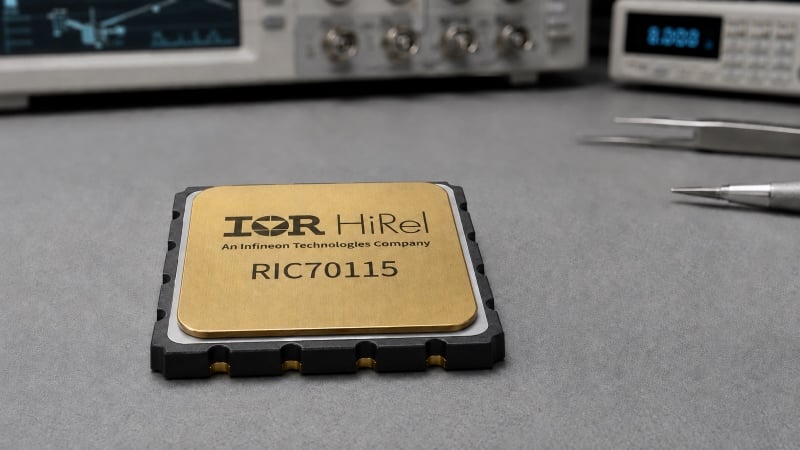
Infineon’s RIC70115 is a radiation-hardened gate driver developed for GaN and silicon power stages in high-reliability satellite systems.
Infineon developed the RIC70115 around that less visible part of the design. The radiation-hardened gate driver works with both GaN HEMTs and logic-level silicon FETs and supports high-side as well as low-side configurations. That versatility is useful because satellite power architectures are unlikely to move from silicon to GaN all at once. Some power stages will make the transition earlier than others.
Radiation Hardness Is Only the Starting Point
The RIC70115 operates across the full military ambient-temperature range of -55°C to 125°C and comes in a hermetically sealed, 16-pin ceramic LCC package. Infineon rates it for total ionizing dose up to 100 krad(Si). The device has also been characterized for single-event effects at a linear energy transfer of up to 81.9 MeV·cm²/mg.
Specifications like these can become a blur on a data sheet, but they address two different problems. Total dose accumulates over the life of a mission. A single-event effect can disrupt a circuit in an instant. The gate driver must tolerate both and still deliver a clean switching signal years after launch.
Radiation performance would mean little if the device compromised the power stage. The RIC70115 can source 1.5 A and sink 2.5 A, giving it the drive strength needed to move charge into and out of the transistor gate quickly. Infineon also specifies low, matched propagation delay with an absolute maximum of 2.9 ns. At GaN switching speeds, small timing inconsistencies can add losses or produce behavior that is difficult to predict. Infineon says it plans electrical screening and qualification to MIL-PRF-38535 Class V for the device.
The TDI Stage Has a Practical Job
GaN’s speed is both its selling point and the source of many gate-drive headaches. A fast edge does not always remain neatly confined to the switch node. Some of that energy can couple into the control path as electromagnetic or radio-frequency interference. The problem becomes harder to manage inside a satellite, where power, control, and communication electronics may be packed into a limited area. Physical separation is not always available as a solution.
The RIC70115 (datasheet linked) handles the input as a differential pair through its Truly Differential Input (TDI) stage. Noise appearing on both lines is treated as common mode interference and rejected, while the voltage difference carrying the intended command remains. Put plainly, this reduces the chance that coupled noise will be mistaken for a genuine switching event.
Removing Some of the Support Circuitry
Noise rejection is only one part of the RIC70115. Infineon has also brought several functions normally placed around the driver onto the chip itself. The integrated low-dropout regulator produces a regulated 4.8-V, gate-drive supply from either a 5-V or 12-V source. Its power-input range extends from 4.75 V to 15 V, allowing it to work with several common bias-supply arrangements without requiring a separate regulator solely for the gate driver.
An independent Miller Clamp handles another familiar problem in fast power stages. A rapid change in drain voltage can push current through the transistor’s Miller capacitance, lifting the gate voltage of a device that should remain off. If the voltage rises far enough, the transistor can turn on unintentionally. The integrated clamp gives that current another path and helps hold the device off during the transition.
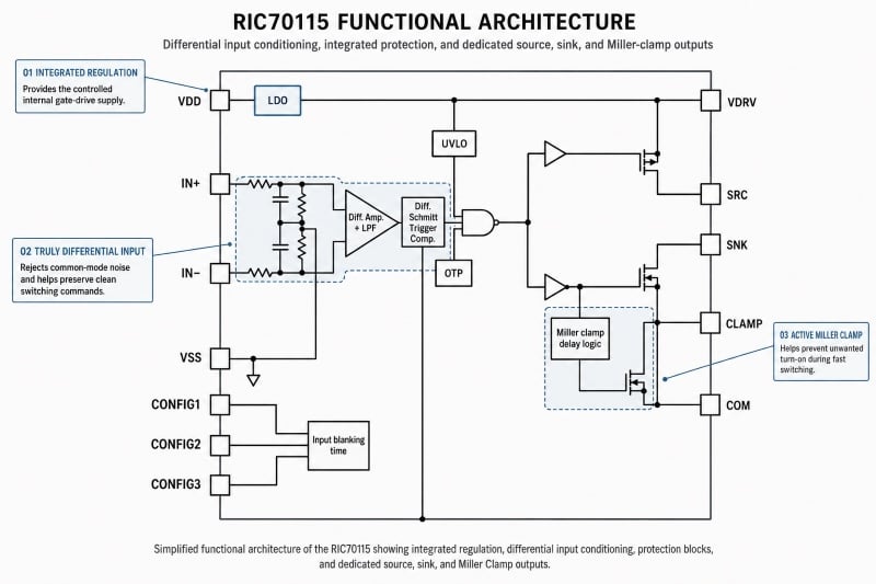
The RIC70115 architecture combines a 4.8-V LDO, undervoltage lockout, TDI input stage, dedicated source and sink outputs, and independent Miller Clamp circuitry.
The LDO, TDI stage, and Miller Clamp do not eliminate every external component. They do, however, remove several support blocks that would otherwise need to be selected, connected, and qualified separately. Fewer parts can simplify the layout and reduce potential failure points.
Where the RIC70115 Fits
Infineon targets the new gate driver at satellite bus and payload equipment, including power-conditioning units, power-distribution units, and DC-DC converters. These are natural candidates for GaN because efficiency and power density gains can directly affect the size and performance of the overall power system.
The RIC70115 is not defined by one headline specification. Its value comes from putting the input stage, regulated gate supply, output drive, and protection functions into a radiation-hardened package that can control either GaN or silicon devices. Moving a satellite power platform from silicon to GaN is rarely a clean break. One converter or power rail may change long before the rest of the system does. Supporting both transistor technologies gives the RIC70115 a place in that stage-by-stage transition.
All images (modified) used courtesy of Infineon.