Rugged 600V 3-Phase Gate Driver with Integrated Bootstrap Diode and Fast Over-current Protection
This article highlights STMicroelectronics STDRIVE601 monolithic device embedding three half-bridge gate drivers for N channel power MOSFETs or IGBTs.
Ruggedness and low cost of ownership over a long service life make three-phase motors, whether they’re induction or permanent-magnet brushless motors, favorites for industrial use. Simpler and cheaper brushed and single-phase motors are increasingly being replaced by three-phase motors in home appliances, boosted by the ongoing demand for high efficiency, clean and quiet operation, and smaller size and lighter weight.
Three-phase motors require a three-phase inverter, which is generally composed of 6 power transistors (MOSFETs or IGBTs), one or more gate drivers to control each power transistor, and control logic (a microcontroller or microprocessor) that implements the control algorithm (speed control, torque control, etc.).
The gate driver is the analog bridge between the digital control and the power actuators and must be reliable, robust against noise and disturbances, accurate (to make the control algorithms and the pulse-width-modulation effective), and in some cases implements protections and safety functions to guarantee safe operation even in unusual conditions or during failures of some parts of the system.
The STMicroelectronics STDRIVE601 is a monolithic device embedding three half-bridge gate drivers for N channel power MOSFETs or IGBTs. It is fabricated using ST’s BCD6s-OFFLINE technology process, which integrates Bipolar, CMOS, and DMOS devices on the same chip, along with floating sections with breakdown voltage in excess of 600 V that can drive the high-side transistors., The new generation BCD6s technology also assures best-in-class ruggedness of the device.
The device includes several auxiliary functions and features to accelerate the design of the system, minimize the need for external components and circuits, avoid using complex and delicate protection schemes against noise and disturbances, and keep the overall application simple and cost-effective.
The STDRIVE601
The STDRIVE601 is housed in a space-efficient SO28 package and replaces three half-bridge drivers, enabling a compact PCB layout. Its 6 outputs can each sink 350 mA and source 200 mA, with gate-driving voltage ranging between 9 V and 20 V.
The 3 high-side bootstrapped sections can operate as high as 600 V and can be supplied through the integrated bootstrap diodes, which save the PCB area and reduce the bill of materials. An under-voltage lockout (UVLO) on the low-sides and each of the high-side driving sections prevent the power switches from operating in low-efficiency or dangerous conditions.
Thanks to technology evolution and design optimization, the STDRIVE601 provides state-of-the-art ruggedness against negative voltage spikes in excess of 100 V and responds quickly to logic inputs in a class-leading 85 ns. Matched delays between the low-side and high-side sections eliminate cycle distortion and allow high-frequency operation while interlocking and deadtime insertion prevent cross conduction under unforeseen conditions.
Smart ShutDown Circuit
Effective overcurrent protection is assured by the smart ShutDown circuit, high-speed protection that turns OFF the gate-driver outputs just 360ns after detecting an overload or short-circuit condition. Designers can set and adjust the duration of the protection OFF-time by changing the value of an external capacitor, without affecting the turnoff reaction time. An active-low fault indicator pin is provided.
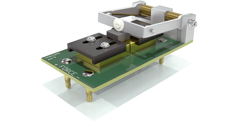
ST also offers the EVALSTDRIVE601 evaluation board to help users explore the features of the STDRIVE601 and quickly get first prototypes up and running.
The Below-ground Voltage Phenomenon
The negative spike voltage of a half-bridge output is often found in power applications, especially if space or mechanical constraints do not allow an optimized PCB layout. The below-ground spike can lead to unwanted phenomena such as the over-charging of the bootstrap capacitor and the incorrect operation of the output stage if devices with insufficient ruggedness are used.
Half-bridge Topologies
In half-bridge topologies, especially when driving highly inductive loads, the output of the power half-bridge could experience a negative voltage, with an initial dynamic spike followed by a static component (Figure 1). This phenomenon occurs when the bridge makes a hard switching transition towards the low voltage level and the load current is outgoing (from the bridge to the load). When the high-side switch turns OFF, the inductive component of the load tries to keep the output current constant. The output voltage drops and when it reaches the “ground” value the current starts flowing through the low-side freewheeling diode, which gets forward biased.
PCB Parasitic Inductances in Series
The main contributors to dynamic below-ground voltage are the spikes due to the high dI/dt experienced by the PCB parasitic inductances in series with the freewheeling diode located along the low-side current path of the half-bridge. Other contributors are the forward peak voltage of the low-side freewheeling diode, which passes from a high voltage reverse condition to a forward condition in a short time and by the parasitic inductance of the shunt resistors.
The static below-ground is mainly due to the voltage drop on the sense resistor (if present) and the forward voltage of the free-wheeling diode (Figure 1).

Figure 1: Below-ground phenomenon in half-bridges
Gate Driver Ruggedness
A key feature of the STDRIVE601 design is its exceptional ruggedness against noise, disturbances and below-ground phenomena. Thanks to the innovative level-shifter architecture and ST’s advanced fabrication process technology, the driver achieves unsurpassed immunity to deep below-ground spikes and properly operates in presence of very steep common-mode transients.
Immunity to below-ground spikes has been tested and confirmed in a dedicated test setup (Figure 2), designed to artificially produce negative spikes much larger than those found in actual applications.
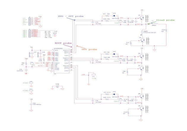
Figure 2: Setup used to analyze the below-ground phenomenon
We’ve driven an RL load (200µH, 16Ω) while putting an inductor with several selectable values (0.19 µH, 0.45 µH, 0.82 µH) in series with the low-side IGBT, to simulate a stray inductance that can be due to very bad PCB layout.
Figure 3 shows the case of a stray inductance of 0.82µH: the output swings from 300V to 0V and the below-ground spike has a minimum peak at -127V and remains negative for about 148ns.
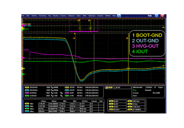
Figure 3: 127 V Below-ground observed on channel 1 output with a stray inductance of 0.82 µH.
Several commutations have been repeated and no damage or malfunction affects the driver.
Bootstrap Diode
The STDRIVE601 internal bootstrap diodes, implemented with 600V rated MOSFETs, charge the bootstrap capacitor of each channel from the main supply voltage (VCC) each time the LVG output is turned ON. This avoids expensive and big external high-voltage diodes.
The integrated bootstrap structure starts conducting immediately on the forward bias, without the typical offset voltage given by actual diodes. This difference is visible from the I-V curve in Figure 4, which shows the transfer curve of an STDRIVE601 bootstrap diode compared with a traditional bootstrap diode. This characteristic gives an immediate benefit in residual voltage drop for a given current and results in charging the bootstrap capacitors even when the voltage drop is small, where the traditional diodes show their limit
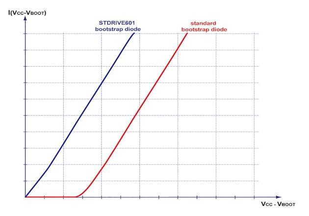
Figure 4: STDRIVE601 bootstrap diode vs standard bootstrap diode
Smart ShutDown Overcurrent Protection
STDRIVE601 integrates a comparator committed to fault protection through a smart ShutDown (SmartSD) circuit.
The SmartSD architecture turns OFF the gate driver outputs in case of overload or overcurrent conditions, with just 360ns delay between fault-detection and the actual output switch-OFF. The protection intervention time, which is about two times faster than other gate drivers in the market, is independent of the duration of the disable time after the fault.
This allows the designer to increase the duration of the output disable time after the fault event up to very large values without increasing the delay time of the protection. The duration of the disable time is determined by the values of the external capacitor COD and of the optional pull-up resistor connected to the (OD) pin (Figure 5).
The comparator for smart ShutDown has an internal voltage reference VREF connected to the inverting input, while the non-inverting input is available on the CIN pin. The comparator’s CIN input can be connected to an external shunt resistor to implement a fast and simple overcurrent-protection function. The comparator’s output signal is filtered from glitches shorter than a fixed time (tfCIN, approximately 300ns) and then fed to the SmartSD logic.
The VREF threshold typical value is 460mV; the comparator input (CIN) has a hysteresis of about 70mV. If the impulse on the CIN pin is higher than VREF, the SmartSD logic is triggered and immediately sets all the driver outputs to low-level (OFF). At the same time, the diagnostic pin (FAULT) is forced low to signal the event (for example to a microcontroller input) and OD starts to discharge the external COD capacitor used to set the duration of the output to disable time of the fault event. As soon as the output disable time expires, the FAULT pin is released and driver outputs restart following the input pins.
Overall Disable Time
The OD unlatch time (t1 in Figure 5), which is the time required to discharge COD capacitor down to VSSDl threshold. The discharge starts as soon as the SmartSD comparator is triggered.
The OD Restart time (t2 in Figure 5), which is the time required to recharge the COD capacitor up to the VSSDh threshold. The recharge of COD starts when the OD internal MOSFET is turned-OFF, which happens when the fault condition has been removed (CIN < VREF - CINhyst) and the voltage on OD reaches the VSSDl threshold. This time normally covers most of the overall output disable time.
If no external pull-up is connected to OD, the external COD capacitor is discharged with a time constant defined by COD and the internal MOSFET’s characteristic (Equation 1), and the Restart time is determined by the internal current source IOD and by COD (Equation 2).
$$t1 \cong R_{ON_{OD}} \cdot C_{OD} \cdot ln \left ( \frac{V_{OD}}{V_{SSDI}} \right )$$
Equation 1
$$t2 \cong \frac{C_{OD} \cdot V_{SSDh}} {I_{OD}} \cdot ln \left ( \frac{V_{SSDI} - V_{OD}}{V_{SSDh} - V_{OD}} \right ) $$
Equation 2
Where VOD = OD floating voltage level
In case the OD pin is connected to VCC by an external pull-up resistor ROD_ext, the OD discharge time is determined by the external network ROD_ext, COD and by the internal MOSFET’s RON_OD (Equation 3), while the Restart time is determined by current in ROD_ext (Equation 4).
$$t1 \cong C_{OD} \cdot \left ( \frac{R_{OD_{ext}} \times R_{ON_{OD}}}{R_{OD_{ext}} + R_{ON_{OD}}} \right ) \cdot ln \left ( \frac{V_{OD} - V_{on}}{V_{SSDI} - V_{on}} \right )$$
Equation 3
$$t2 \cong C_{OD} \cdot R_{OD_{ext}} \cdot ln \left ( \frac{V_{SSDI} - V_{on}}{V_{SSDh} - V_{on}} \right )$$
Equation 4
where
$$V_{on} = \frac{R_{ON_{OD}}}{R_{OD_{ext}} + R_{ON_{OD}}} \cdot V_{CC} ; \ V_{OD} = V_{CC}$$
Figures 6 show examples of Smart ShutDown operation, with two different capacitors connected to the OD pin. The triggering pulse on CIN has a width of 500ns, with amplitude (peak to peak) of 1V; the internal current source (IOD) has been used to charge the external capacitor
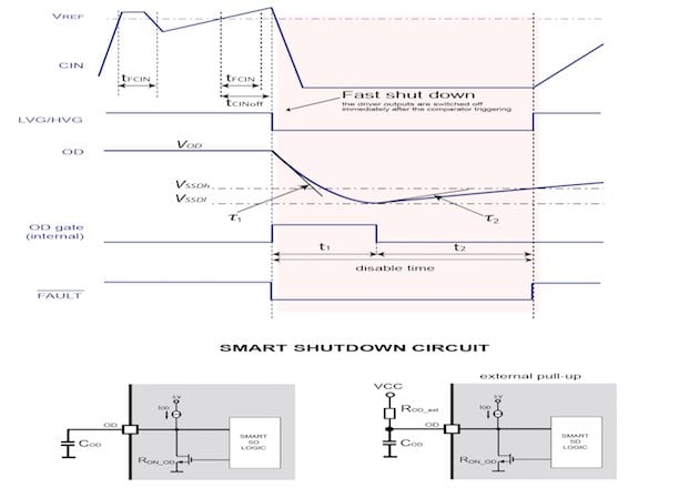
Figure 5: Smart ShutDown timing waveform.
$$disable \ time = \frac{C_{OD} \cdot V_{SSDh}}{I_{OD}} + R_{ON_{OD}} \cdot C_{OD} \cdot ln \left ( \frac{V_{OD}}{V_{SSDI}} \right ) $$
COD = 2.2 µF
⇒ disable time = 1.46 s
VSSDh = 4 V
VSSDl = 0.56 V
IOD = 6 µA
RON_OD = 25 Ω
VOD = 15 V
Cod = 330 nF
⇒ disable time = 220 ms
VSSDh = 4 V
VSSDl = 0.56 V
IOD = 6 µA
RON_OD = 25 Ω
VOD = 15 V
Other Functions and Characteristics
The STDRIVE601 has been designed to have fast and accurate propagation delays. From input toggling to output turn-ON (or OFF), the delay is 85ns for both Low and High-side drivers and the matching time is less than 30ns, with a typical delay matching of 0ns. An UnderVoltage LockOut (UVLO) mechanism monitors the supply voltage of the output stage of the driver and turns it OFF when the voltage drops below a pre-defined threshold. This protection prevents the device from driving the power transistors when the supply voltage is so low that it would lead to high conduction losses or, even worse, transistor damage.

Figure 6: On the first figure COD = 2.2 µF, on the second figure COD = 330 nF
The UVLO threshold has a hysteresis and a built-in filter to prevent unwanted activations from noise on the supply voltage. All 6 drivers in STDRIVE601 are protected by the UVLO mechanism.

Figure 7: UVLO mechanism on VCC power supply
With the many advantages of three-phase motors, they are rapidly displacing simple single-phase and brushed motors. The ease of use, availability, and cost-effectiveness of three-phase inverters, like the STDRIVE601, which is a three-phase 600V-rated single-chip gate driver, is a valuable contributor to this progress. The STDRIVE601 delivers the robustness, simplicity, and cost-saving while assuring protected system and safety functions.
About the Authors
Michele Lauria received his Masters of Electronic Engineering at the Polytechnic University of Milan and worked as a Senior Application Engineer at STMicroelectronics, which is a global semiconductor leader delivering intelligent and energy-efficient products and solutions that power the electronics at the heart of everyday life.
Massimiliano Magni worked at STMicroelectronics in which a global semiconductor leader delivering intelligent and energy-efficient products and solutions that power the electronics at the heart of everyday life.
This article originally appeared in the Bodo’s Power Systems magazine.