Facebook
 Google
 GitHub
 Linkedin
Rethinking Isolation in AI Factories for High-Density Power Conversion
AI factories are moving to 800 VDC to manage power demands, complicating isolation. Integrated gate drivers solve this by merging signal and power.
Article co-authored by Allegro's Anna Chiu.
Generative AI is changing more than computing hardware inside the data center. It is rewriting the rules of power delivery and forcing engineers to reconsider how power is converted, distributed and protected—from the utility connection to the processor.
AI accelerators consume far more power than the server processors they replace. NVIDIA's Hopper H100 is rated at around 700 W, while the Blackwell B200 rises to approximately 1,200 W and the Blackwell Ultra B300 reaches about 1,400 W. Across tightly packed GPU trays, this creates a step change in rack power density. Systems such as the GB200 NVL72 already reach 120 kW to 132 kW, and future AI factories are expected to go further.
That increase creates a physical problem. Delivering 120 kW over a conventional 54 VDC rack bus requires more than 2,200 A. Conductors carrying that level of current consume space, add weight and generate resistive heat. In some high-density designs, copper busbars can approach 200 kg. The limitations are mechanical and thermal as well as electrical.
The industry response is a move toward 800 VDC distribution. Raising the voltage by almost a factor of 15 delivers the same power at a fraction of the current. It can reduce copper requirements by approximately 45% to 50% and, because resistive losses scale with current squared, cut I2R losses by more than two orders of magnitude.
Yet 800 VDC is not simply a substitute bus voltage. It changes the power-system architecture and places new demands on the converters, switches and isolation technologies that make the transition possible (Figure 1).
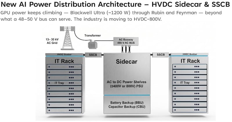
Figure 1. As supplies scale toward 30 kW and beyond, higher bus voltages and density targets push designers toward more complex multi-level architectures.
Higher Voltage Changes Converter Architecture
At lower power levels, conventional single-stage topologies can meet efficiency, thermal and power-quality targets. As supplies scale toward 30 kW and beyond, higher bus voltages and density targets push designers toward more complex multi-level architectures.
For example, T-type neutral-point-clamped (NPC) power factor correction (PFC), Vienna PFC and flying-capacitor multiphase buck/boost divide the input voltage across multiple switching devices. This reduces device stress and switching loss, helping exploit silicon carbide (SiC) MOSFETs and gallium nitride (GaN) HEMTs. The trade-off is more switches and control complexity.
A T-type NPC PFC stage can expand a six-switch arrangement to 12 active devices. It may require six isolated gate drivers for the boost switches and three for bidirectional back-to-back switches. Because these devices float at different high-voltage potentials, their gate drives cannot share a ground reference.
The result is a proliferation of isolated power domains. A conventional implementation may require seven isolated bias supplies for the PFC stage alone. With an interleaved LLC DC-DC converter downstream, a 30-kW supply can require up to 18 isolated bias rails, 18 non-isolated rails and 54 isolation barriers (Figure 2).
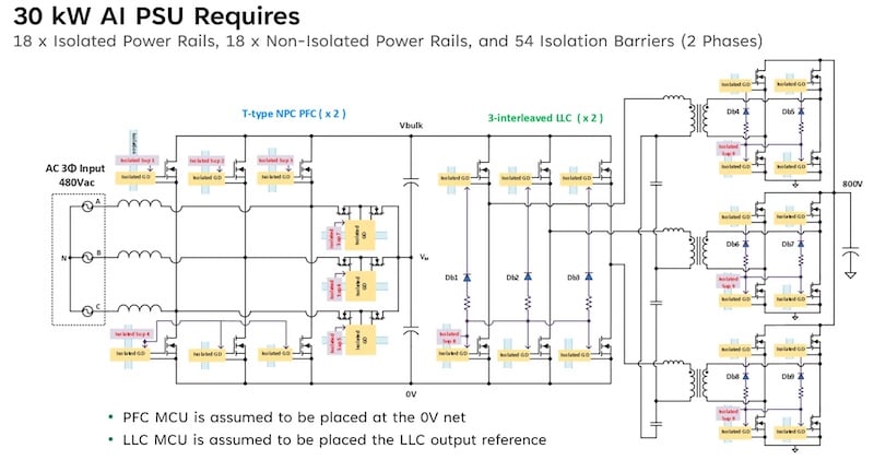
Figure 2. 30 kW supply requirements include up to 18 isolated bias rails, 18 non-isolated rails and 54 isolation barriers.
The challenge is therefore not only efficient conversion. Designers must also deliver reliable control power and switching signals to many floating devices without surrendering the space saved elsewhere.
The Hidden Cost of Isolation
Every isolated gate driver needs a control signal and power on the isolated side. Conventionally, the signal crosses a digital isolator or isolated driver, while a transformer-based DC-DC circuit generates the floating supply.
Across dozens of switches, these circuits become a substantial part of the design. Each domain may need a controller, transformer, rectification, regulation and protection. Negative turn-off supplies for SiC and high-side bootstrap networks add more components.
The constraint is particularly severe in a 1U power shelf. Although a rack unit is 44 mm high, usable board height may be closer to 30 mm after chassis, airflow and clearance allowances. Discrete transformers and bias circuits compete with semiconductors, magnetics, capacitors, control electronics and cooling.
Crowding also affects switching performance. Longer gate and power loops increase parasitic inductance, producing gate-voltage ringing, unintended turn-on and switch-node overshoot. Layout becomes part of the switching system rather than a secondary packaging consideration.
Isolation transformers introduce another issue that becomes more important as switching speeds rise: parasitic capacitance between their primary and secondary windings.
When Fast Switching Becomes Common-Mode Noise
Wide-bandgap devices are central to the 800 V architecture because they switch with lower losses and at higher frequencies than silicon. This shrinks magnetic components and improves density. However, voltage slew rates of 100 V/ns or more can turn small parasitic capacitances into significant common-mode current paths.
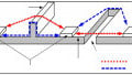
Common-mode current equals isolation capacitance multiplied by the rate of change of voltage. A conventional isolated bias transformer may exhibit 10 pF to 30 pF of primary-to-secondary capacitance. At 100 V/ns, 30 pF produces a transient current of 3 A whenever the switch node changes state (Figure 3).
$$I_{CM} = C_{CM} \times ( \frac{dv}{dt})$$
That current crosses the barrier, enters the low-voltage control domain and returns through the PCB ground structure and bulk capacitors. It can cause ground bounce, corrupted PWM signals, false switching and controller resets. Charging and discharging the capacitance also adds switching loss.
Shielding, common-mode chokes and larger EMI filters can control these effects, but they add cost and volume and work against the goal of higher power density. Isolation becomes both a space issue and a noise problem.
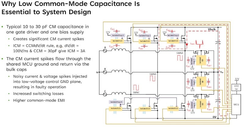
Figure 3. Typical 10- to 30-pF common-mode (CM) capacitance in a gate driver and bias supply creates significant CM current spikes that flow through the shared MCU ground and return via bulk capacitors. The noise and voltage spikes injected into the low-voltage control ground plane results in faulty operations and higher switching losses and commode-mode EMI.
Integration Changes the Gate-Drive Equation
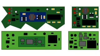
A different approach is to combine isolated signal transmission and isolated bias power within a single surface-mount gate-driver package. Rather than relying on bulky external components for separate data and power paths, the device integrates high-speed signal isolation and an isolated bias power supply into a single, compact surface-mount package.
Integration removes much of the external bias circuitry associated with each floating switch. A discrete isolated DC-DC controller and transformer are no longer required, while secondary regulation, bias splitting, bootstrap components and protection networks can be reduced. Across many floating domains, board-space savings can exceed 50%.
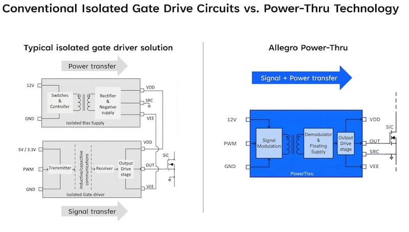
Figure 4. A conventional isolated gate-driver architecture with a separate bias supply, compared with an integrated signal-and-power approach.
The value of integration extends beyond component count. A power-transfer structure developed at IC scale can be optimized for much lower coupling capacitance than a conventional transformer. With approximately 2.2 pF of isolation capacitance, common-mode current at 100 V/ns falls to about 0.22 A, compared with 3 A through a 30-pF transformer.
That 10-fold to 15-fold reduction changes the noise environment around the driver. Less transient current reaches controller ground, improving signal integrity and reducing false-trigger risk. It can also ease common-mode filtering and EMC qualification without sacrificing the space gained through higher-voltage distribution.
Integration also simplifies isolation planning. A traditional half bridge may require several physical boundaries between the low-voltage controller, floating high-side circuitry and power stage. Bringing the signal, isolated power and output stage into one package consolidates much of this complexity around a single reinforced barrier.
The PCB designer can place the driver close to the SiC or GaN switch, shorten the gate loop and reduce parasitic inductance. Creepage and clearance still govern the layout, but there are fewer transformers and floating supplies to position, producing a more repeatable design across converter channels.
These advantages are especially relevant to 30 kW power shelves, where multi-level PFC and interleaved DC-DC stages combine high switch counts with strict thermal and mechanical constraints. Integrated drivers do not remove the topology's complexity, but they prevent the supporting architecture from multiplying at the same rate as the power stage.
Beyond the Power Supply
The implications of 800 VDC extend beyond the power supply unit (PSU). A high-voltage distribution backbone also requires fast and reliable protection before power enters the compute rack, driving interest in solid-state circuit breakers (SSCBs) capable of interrupting DC fault currents in microseconds.
Unlike AC, a DC bus has no natural current zero crossing to help extinguish an arc. An 800 VDC fault must be interrupted rapidly enough to protect cables, busbars and downstream equipment. A practical solid-state circuit breaker may use parallel SiC MOSFETs to reduce conduction loss and handle the current, creating further floating gate-drive and thermal challenges.
A conventional SSCB can require a dedicated isolated DC-DC converter and multiple barriers. An integrated driver generates its own floating turn-on and negative turn-off supplies, removing much of the external bias circuit. In a system measured in microseconds, the driver must switch cleanly without noise-induced delay or unintended operation.
The same isolation technologies can also support battery interfaces and high-power DC-DC conversion. As 800 VDC moves deeper into the data hall, the number of places requiring compact, low-capacitance isolation will continue to grow.
Preparing for the AI Factory
AI infrastructure is approaching a point where power architecture will determine how quickly computing capacity can scale. Low-voltage distribution cannot absorb ever-higher rack power through larger conductors and more aggressive cooling. Moving to 800 VDC offers a route past that constraint, provided conversion and protection systems meet demanding efficiency, density, reliability and EMC targets.
Integrated isolated gate drivers are one enabling element. By combining signal isolation and bias power, they reduce components around each floating switch, lower common-mode capacitance and simplify high-voltage PCB layout. The benefits grow as multi-level converters increase the number of independently referenced devices.
Allegro's Power-Thru technology applies this approach to isolated gate drivers for GaN and SiC power stages. Instead of treating the bias supply as a separate subsystem, it brings power and signal transfer into one device. For engineers building high-density PSUs and solid-state protection, that means a smaller footprint, quieter switching and a more direct path from prototype to qualified hardware.
The transition to the 800 V AI factory will not be defined by a single component or topology. It will depend on coordinated advances across power semiconductors, magnetics, sensing, cooling, protection and control. But as rack power rises and isolation domains multiply, delivering clean power and control across every high-voltage boundary will be fundamental. Smart integration turns that boundary from a growing design burden into a practical building block for the next generation of AI infrastructure.
All images used courtesy of Allegro Microsystems.