Facebook
 Google
 GitHub
 Linkedin
Overcoming the Challenges of Characterizing High Speed Power Semiconductors
This article discusses DPT fixture design to obtain repeatable and reliable results from a DPT setup.
Having trouble obtaining consistent results from your Double-Pulse Test (DPT) setup? You are not alone. As the switching frequency of switch-mode power converters increases into the MHz range, rise/fall times can drop to 10ns or even single digits of nanoseconds. It is no longer possible to design & measure power converter performance without considering high-frequency effects. This article discusses DPT fixture design to obtain repeatable and reliable results from your DPT setup.
International Electrotechnical Commission (IEC) and JEDEC standards have existed for decades, defining tests to dynamically characterize power semiconductors. The DPT setup is the industry standard for measuring and extracting most of the key dynamic parameters to characterize these devices (Figure 1).

Figure 1: Basic Double-Pulse Test Configuration.
These standards were sufficient for slower switch mode power converters because BW requirements of measurement equipment and fixturing connecting to the power semiconductor DUT were obtainable with standard low-frequency power design practices and measurements. The switching frequencies of power converter designs were in the kHz to 10s of kHz range, not requiring extensive high-frequency analysis or design.
With many power converter markets (e.g. automotive and alternative energy) pushing for a reduced cost, higher efficiency, higher voltages, and better thermal performance, the pressure on the power semiconductor industry has driven faster Si-based switching capabilities (Si MOSFETs and IGBTs) as well as the emergence of Wide Bandgap (WBG) semiconductor technologies, specifically Silicon Carbide (SiC) and Gallium Nitride (GaN).
To investigate the reason for more difficulty in making DPT measurements with faster switching devices, let’s refresh our memory of the mathematical relationship between rise time and bandwidth.
The basic formula relating the bandwidth of a pulse waveform to its
$$t_r \approx \frac{K}{f_{3dB}}$$
Where:
tr = pulse rise time (10% - 90%)
f3dB = 3 dB bandwidth
K = constant of proportionality depending on pulse shape
(assume 0.35 for single-pole exponential decay)
For determining the impact of the parts of the DPT measurement system (e.g. scope, probe, fixture, and DUT), we use the following formula to determine the risetime that would be displayed on the oscilloscope:
$$t_{displayed} = \sqrt{t^2_{DUT} + t^2_{DPT \ fixture} + t^2_{probe} + t^2_{scope}}$$
Armed with these relationships, let’s compare two scenarios to illustrate the change in expectation for high-frequency consideration.
Scenario #1: Analyze the impact of a 10 kHz switching waveform from an Si power MOSFET with 0.2 µs rise times. Because mid-range oscilloscope bandwidths are typically 500 MHz or more and their associated voltage probes can have bandwidths of 300 MHz, let’s assume these common bandwidths for this scenario. Let’s also assume that DPT fixture was designed with low-frequency considerations and provides a 20 MHz bandwidth.
$$t_{displayed} = \sqrt{ \left( 0.2 \times 10^{-6} \right)^2 + \left( \frac{0.35}{20,000,000} \right)^2 + \left( \frac{0.35}{300,000,000} \right)^2 + \left( \frac{0.35}{500,000,000} \right)^2} $$
$$t_{displayed} = 0.2008 \times 10^{-6} \ sec $$
Result: The displayed value on the oscilloscope is very close (< 1% error) to the actual rise time of the MOSFET, with little to no impact from the DPT fixture, probe or oscilloscope.
Scenario #2: Analyze the impact of a 250 kHz switching waveform from a SiC power MOSFET with 10 ns rise times. Let's assume the same situation above for the oscilloscope (BW = 500 MHz), voltage probe (BW = 300 MHz), and the DPT fixture (BW = 20 MHz).
$$t_{displayed} = \sqrt{ \left( 10 \times 10^{-9} \right)^2 + \left( \frac{0.35}{20,000,000} \right)^2 + \left( \frac{0.35}{300,000,000} \right)^2 + \left( \frac{0.35}{500,000,000} \right)^2} $$
$$t_{displayed} = 20.2 \times 10^{-9} \ sec $$
Result: The displayed value on the oscilloscope has slightly more than a 100% error! Let’s run scenario #2 again with a DPT fixture designed for a 200 MHz BW and see how much impact that will have on the result.
$$t_{displayed} = \sqrt{ \left( 10 \times 10^{-9} \right)^2 + \left( \frac{0.35}{200,000,000} \right)^2 + \left( \frac{0.35}{300,000,000} \right)^2 + \left( \frac{0.35}{500,000,000} \right)^2} $$
$$t_{displayed} = 10.2 \times 10^{-9} \ sec $$
Result: The displayed value on the oscilloscope has only a 2% error. This is a significant improvement in results by designing the fixture for a 200 MHz bandwidth.
Common instruments, like oscilloscopes, are more than capable to support the needs of a high-speed DPT system. More significant challenges to providing repeatable and reliable results involve the design of the DPT fixture, including the connection of the measurement probes.
NOTE: Because our analysis involves 2 poles, we must consider the relationship between rise time and bandwidth for second-order systems. Simple second-order circuit simulation was performed to approximate the ratio. The graphed result shows the tr *f3dB product to be close to 0.35 for (0.5 < ζ < 1.0). And for (0.05 ζ < 0.5) the ratio only drops to ~0.27. Therefore, our conclusion remains valid for second-order systems. [2]
Considerations for DPT Fixture Design
Because of the faster rise/fall times (i.e. higher bandwidths) required for newer power semiconductors, analysis of the fixture layout and circuit parasitics are critical to providing repeatable and reliable DPT waveforms. If not, DPT waveforms often have second-order underdamped oscillations of the pulsed waveforms (VGS, VDS, ID), making it impossible to extract repeatable dynamic characterization parameters (e.g. e(on), e(off)) (Figure 2).

Figure 2: Turn off pulses from a GaN device (VDS=100V, I D=10A, VGS=12V).
Figure 3 shows the DPT setup with the primary parasitics capacitances, inductances, and resistances that need to be considered when designing your DPT fixture. Some of these parasitics are inherent in the power devices themselves (e.g. Cgd, Rg, Ls). Power semiconductor manufacturers continue to develop new packaging materials and designs to minimize the stray parasitics. Once you determine your power semiconductor of choice, the focus is on external parasitics within the fixture.

Figure 3: Primary parasitics needing consideration during DPT switching transients.
There are three loops that are worth considering when analyzing the Double-Pulse waveforms (VGS, VDS, ID): the DC-Link Loop, the Gate Loop, and the Power Loop (Figure 3). As always, it is good practice to minimize the area of the loop, which is proportional to the total loop inductance. This can be done practically by routing PCB traces (main and return) close to each other, or by using twisting pairs if routing the signals through wires.
The DC-Link Loop should be considered when the DC-Link Capacitor, that is charging the load inductor (L), is interrupted (i.e. when the DUT is turned off). When the DUT is turned off, the current charged up in L recirculates through the body diode in the high-side MOSFET. Therefore, there is no current coming from the DC-Link Capacitor and the DC-Link stray inductance (LDC-Link) has a large -di/dt. LDC-Link resonates with the Decoupling Capacitor in parallel with parasitic output capacitance from the half-bridge, developing a voltage surge across VDC and VDS. This resonant oscillation can be seen on VDS in Figure 4 during both turn-off events. It can also be seen in Figure 2 as the lower frequency oscillation of VDS. It is next to impossible to eliminate this oscillation, but care needs to be taken to minimize it.

Figure 4: Double-Pulse Test Waveforms (SiC MOSFET, 1200V, 40A).
For the Gate Loop, the main parasitics you have control over in your fixture layout are LGL and LPL2. It is often not possible to minimize this inductance enough to prevent oscillation, depending on the DUT’s gate resistance (Rg). If the oscillation still exists, then an external gate resistor RG is required to dampen the oscillation to enable repeatable parameter extraction. Unfortunately, the trade-off in adding resistance to the gate is a slower rise time of the gate voltage.
SiC geometries are typically much smaller than Si, and therefore often have larger internal gate resistance (Rg). So, it may not be necessary to add external gate resistance to some SiC devices to dampen the oscillation. While Si MOSFETs may require external dampening, because of the smaller Rg. One often finds many different gate resistor values used in DPT systems to accommodate the specific power device being characterized.
The Power Loop parasitics are another source of oscillation in VDS and ID. After ramping the current to the desired value in L, during the first of the two pulses, the DUT is turned off. The current in L is recirculated through the body diode. The -di/dt in the power loop inductance (LPL1), creates a voltage surge across the drain and source of the DUT. This voltage surge resonates with Cds of the DUT and the parasitic inductance of the Power Loop (LPL1), creating a higher frequency oscillation that can be seen in VDS and ID in Figure 2. Although mechanisms are slightly different from turn-on, LPL1 continues to be the key parasitic involved. Additionally, with WBG devices having low Rds(on) values, damping of the Power Loop is minimal. Unfortunately, this often means limiting switching speeds to minimize oscillations.
There is one other mechanism that impacts the switching performance of the DUT. This mechanism is caused by the common parasitics (Cgd and LPL2) in both the Power Loop and the Gate Loop (Figure 5). For the high di/dt events (turn-on and turn-off), the common inductance LPL2 creates a back EMF, which minimizes the effective VGS in the Gate Loop.

Figure 5: Power Loop parasitics minimizing Gate Loop drive.
It is sometimes possible to see the ringing of the power loop superimposed on the VGS due to this coupling (Figure 2). Similarly, the high dv/dt events (turn-on and turn-off) create a displacement current in the Miller Capacitance (Cgd) diverting gate current intended to charge Cgs. This result also negatively impacts the effective VGS and the ability to quickly turn-on the DUT. Both effects impact the consistency and speed of the switching transition of the DUT. DPT fixture design is quite a challenge, and as we’ve seen, it becomes significantly more difficult as rise/fall times continue to decrease. One needs to consider high-frequency effects of multiple second-order circuits (loops) and is often limited in the ability to minimize parasitic inductances and capacitances. Fundamental technology barriers (e.g. low inductance interconnects) exist in designing and constructing DPT systems to characterize newer power semiconductors

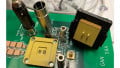
Figure 6: PD1500A DPT Modular fixture.
However, the Keysight PD1500A Dynamic Power Device Analyzer/ Double-Pulse Tester was developed to solve these tough problems. The PD1500A is a complete DPT system designed for Si and SiC-based discrete power semiconductors. The system was architected to be modular and upgradeable as the market evolves to higher voltages and frequencies. Keysight has plans for additional versions to characterize power modules, GaN devices, and to provide some reliability testing (Short Circuit, Avalanche). Just as you’ve come to expect from the B1505/6A Device Power Analyzers, the PD1500A provides repeatable and reliable results (see typical waveforms in Figure 4).
The PD1500A’s carefully engineered, modular fixture minimizes unwanted parasitics (Figure 6). Multiple gate driver options are provided with some standard resistor values, as well as an option for customer supplied resistors. DUT boards for TO-247 and SMD D2PAK-7 footprints and Si MOSFET, IGBT, and SiC devices are also provided. Additional gate driver and DUT board options will be provided in the future.
About the Authors
Ryo Takeda worked as a business development engineer at Keysight Technologies Incorporated, a company driven to deliver breakthrough solutions and trusted insight in electronic design, test, manufacture, and optimization to help customers accelerate the innovations that connect and secure the world.
Bernhard Holzinger worked at Keysight Technologies Incorporated, a company driven to deliver breakthrough solutions and trusted insight in electronic design, test, manufacture, and optimization to help customers accelerate the innovations that connect and secure the world.
Mike Hawes is the automotive and energy solutions planning manager at Keysight Technologies. holds a Master's Degree in Biomedical Engineering at Colorado State University. He also holds a Bachelor's Degree in Electrical Engineering at Washington State University.
References
- H. W. Johnson, M. Graham, “High Speed Digital Design – A Handbook of Black Magic”, Prentice Hall PTR, Englewood Cliffs, New Jersey 07632, 1993, pp. 8-10, 399.
- M. T. Thompson, “Intuitive Analog Circuit Design”, Elsevier Inc., Second edition, 2014, pp. 35-37.
This article originally appeared in Bodo's Power Systems magazine.
Related Content