Facebook
 Google
 GitHub
 Linkedin
Improving Vacuum Solder Reflow for Challenging Power Module Packaging
This article discusses the evaluation of flux-free soldering process for bare copper DBC substrate to Nickel-plated copper base plate soldering.
The Power Module Packaging Market is projected by some analysts to have a CAGR of nearly 10% from 2019 through 2025, driven by the competing demands for more global energy consumption and the push to reduce the impact of fossil fuels on our environment. Sustainable energy and savings through improved efficiencies will drive improvements in the chip and packaging technologies used in power electronics.
Increased energy consumption worldwide means an increased need for power electronics devices to meet the requirements along the electrical energy supply chain, from generation to consumption. These devices are required to be more efficient and to operate under more stressful conditions, such as higher temperatures and more power cycles. This is particularly true for the automotive industry, as it transitions from fossil-fuel-powered engines to hybrid electric and battery electric vehicles.
Power Modules for the Electric Vehicle Market
Provided the drivers for the growth of the HEV/EV market remain in place, there are tremendous opportunities ahead for power modules and the necessary vehicle charging infrastructure. This growth should continue to be rapid, as evidenced by the investment into EV technologies by many the top car-producing nations. To meet the requirements of the automotive industry, the semiconductors which populate these modules will need to endure higher operating temperatures and have extended service lives.
The rising demand for power modules does not depend strictly on the conversion of passenger vehicles to the electric power train. There are also abundant opportunities in other areas such as elevators, motor converters, solar energy, welding, industrial frequency converters, pumps, large scale medical devices and so on. All benefit from increased efficiency.

Figure 1: Typical power module construction
Power Modules: Typical failure modes
For a conventional IGBT module consisting of a stack-up of materials and interconnects, the interconnects within the package are the source of mechanical failures due to the thermal expansion mismatches that exist between the materials and components in the assembly. Typical failure modes can include wire bond lift-off due to rapid power cycling or cracks in the solder due to temperature changes.
Application Study: Developing a lead-free, flux-free, extremely low void solder attach process
The Baseplate-to-DBC solder attach was selected, as the increased surface areas for this interconnect pose challenges within the assembly operation and are a source of yield loss for conventional reflow systems, often due to high void rates. Achievement of low cumulative voiding over the entire solder joint is difficult due to the large solder joint surface area and the baseplate bowing found in most module designs. If flux is used, this can exacerbate the voiding issue. Plus, there is the added challenge and expense to ensure the flux residue has been cleaned from the product after reflow. The power electronics industry is actively seeking a reliable flux-free solder reflow process that achieves low void rates over increased surface areas. With decades of experience operating in high-reliability microelectronics markets that demand a flux-free, void-free solder reflow process, Palomar Technologies is prepared to deliver similar solutions to the power module industry with its SST Vacuum Reflow Systems.
For this application work, a lead-free alloy, SAC305, 0.100 mm thick, was chosen to comply with the European Union and Japan legislation restricting the use of hazardous materials. This E.U. mandate is known as the RoHS (Restriction on Hazardous Substances) Directive and restricts the use of hazardous substances, including lead, in electrical and electronic equipment.
Sulfamate nickel plating for the 44 mm X 104 mm X 3 mm thick baseplate was selected as it provides a more solder-friendly surface vs. electroless nickel plating, as the increasing phosphorous content used in different varieties can hinder the wetting process. The 24 mm X 28 mm DBC was bare Cu. There are three commonly used metal oxide reduction techniques for electronics assembly.
-
100% or a very high concentration of a hydrogen atmosphere: Effective, but there are safety concerns about using this highly combustible material in the assembly facility.
-
Forming Gas: A Nitrogen/Hydrogen mix, usually in the 95/5 or 97/3 ratio, is safe to use but is not effective unless operating at 350° or higher. If the temperature range is compatible with your materials, then it does effectively reduce the oxide layer on metals such as copper and nickel.
-
Formic Acid: A “low-temp” method to remove the metal oxide layer from surfaces, such as copper or nickel. The power module industry has become very interested in this method. The industry is looking to eliminate the use of flux, but requires an oxide reduction method that is compatible with their materials, that is environmentally friendly, and that is easy to integrate into their existing production process. Formic acid fulfills these requirements.


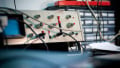
Images 2 & 3: Fixture with three Cu Alumina DBC on top of SAC305 preforms and baseplate; reflowed assembly.
An SST Model 5100 Vacuum-Pressure Reflow System was selected to conduct the application. The SST QuikCoolTM Option was not used for this evaluation. However, it is recommended it be included on a system used for the production of power modules for the following reasons:
-
Productivity improvement: It will increase the throughput by reducing the cooldown portion of the profile.
-
It will reduce the TAL, or time-above-liquidus, which is a factor for intermetallic compound growth at the interface areas.
Description of the Process Profile Used During Evaluation The profile review: The SST Model 5100 with 12" x 12" thermal work zone can include up to six monitoring thermocouples on the assembly to track the temperature during the profile. The vacuum and pressure are monitored at all times. This evaluation profile included:
-
An initial vacuum followed by a nitrogen purge as the means to evacuate the chamber, fixture, and components of the atmosphere, moisture, oxides and other forms of contamination that hinder the reflow operation.
-
Temperature is ramped up to 160°C to start the formic acid process.
-
The formic acid concentration is adjustable. A 6% level was used. Chamber exhaust remains open during the formic acid portion of the profile.
-
The chamber is purged of any remaining fumes by a brief increase in pressure; then a small amount of nitrogen is added to aid the heat transfer as the temperature is ramped up to the reflow peak.
-
At the end of the temperature peak, when the solder is molten, the chamber pressure is increased to 40 PSIG (3.8 Bar) to collapse any remaining voids (air bubbles) trapped in the solder.
-
The chamber remains pressurized during cool down till solder returns to solidus.


Images 4 & 5: CSAM images showing voiding (in red) of sample B55 at T0 and T50 temperature cycles.
| Sample # | Sample ID | T0 Void Rate | T25 Rate | T50 Rate | Comments |
| 1 | B48 | 0.5% | 0.6% | 0.8% | |
| 2 | B49 | 0.5% | 0.5% | 0.5% | |
| 3 | B50 | 0.5% | 0.5% | 0.5% | |
| 4 | B51 | 1.1% | 1.1% | 1.2% | |
| 5 | B52 | 1.6% | 1.6% | 1.7% | Probably due to undercut preform shift |
| 6 | B53 | 1.1% | 1.3% | 1.3% | |
| 7 | B54 | 0.9% | 1.0% | 1.0% | |
| 8 | B55 | 0.3% | 0.3% | 0.3% | |
| 9 | B56 | 0.4% | 0.4% | 0.4% | |
| 10 | B57 | 1.6% | - | - | Used for x-section at T0 |
| 11 | B58 | 0.3% | - | - | Used for x-section at T0 |
| 12 | B59 | 3.1% | - | - | Probably due to undercut preform shift; used for x-section at T0 |
| Average | 0.99% | 0.81% | 0.86% |
Table 1: CSAM Void Rate Calculations
Void Results: Less than 1% Void Ratio
The assembled samples were sent to a 3rd party for void rate calculation through the use of a scanning acoustic microscope (CSAM) and subject to -40° to 125°C. temperature cycling. Table 1 below shows the calculated void rates through the first 50 cycles. The average void rate remains at just below 1% at T0, T25 and after T50 cycles (-40°/+125°C).
Conclusions
The purpose of this study was to evaluate the flux-free soldering process for bare copper DBC substrate to Nickel-plated copper base plate soldering. Using SST’s unique void reduction reflow soldering technology and with the use of formic acid, as a means for surface oxide removal, the low voiding results of less than 1% were demonstrated. The same technique can be applied for soldering of power dies (IGBTs, MOSFETs, and Diodes) to DBC substrates with similar results. Future tests by SST will be conducted using 95Sn/5Sb solder alloy with bond line control features. This should be 64 x 34 mm DBC substrate and a similar base plate to demonstrate similar low-void capabilities.
About the Author
Matt Vorona holds a Master's Degree in International Business Concentration at Columbia University - School of International and Public Affairs and a Bachelor's Degree in Foreign Affairs earned at the University of Virginia. He is competent in direct technical sales and sales management; business development; general management; and P&L and annual budget responsibility. He currently works as the Regional Sales Manager for North America and Europe at SST Vacuum Reflow Systems.
This article originally appeared in the Bodo’s Power Systems magazine.