Facebook
 Google
 GitHub
 Linkedin
High Voltage Family of Controllers Reduces DCtoDC Converter Cost and Size
This article highlights ADI LTC3892 high voltage controllers with an ability to reduce power losses by adjusting the gate voltage of MOSFETs and low IQ.
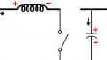
LTC3892 is a versatile controller, widely used in automotive and industrial applications. The main advantages of this controller are the ability to reduce power losses by adjusting the gate voltage of switching MOSFETs and extremely low quiescent current — 3.6μA at shutdown. This is a high voltage family of controllers with an input/output voltage range of 4.5V to 60V. It’s very attractive for industrial customers because it can replace costly, bulky transformers in 48V input rail applications with less expensive, compact step-down converters.
High voltage controllers significantly reduce the cost of automotive electronics in 12V and 24V input rail applications by eliminating external transient and overvoltage protection circuitry, which simplifies the entire design.
Circuit Description and Functionality
Figure 1 illustrates a dual out, step-down converter with VOUT1 5V at 8 A and VOUT2 12V at 5A. It features the LTC3892, a controller that comes in a 32-lead QFN package and that provides the following functions: selection options by the ILIM pin current sense voltage, pin VPRG1 that can set the output voltage to 3.3V or 5.0V without the external resistor divider, and power good pins for both outputs. LTC3892 also provides output overvoltage protection for both channels by turning on the bottom MOSFET in case of overvoltage. This chip provides protection from short-circuit conditions by implementing foldback current limiting.

Figure 1: Electrical schematic of LTC3892 in a dual output dc-to-dc converter where VOUT1 is 5V at 8A and VOUT2 is 12V at 5A.
The power train of the first channel includes MOSFETs Q1, Q4, inductor L1, and an output filter based on CO1. The power train of the second channel includes MOSFETs Q2, Q3, inductor L2, and an output filter based on CO2. The MOSFETs are not logic level and pins DRVUV and DRVSET are tied to INTVCC to provide a 10V gate drive. Pin VPRG1 is tied to INTVCC to select a 5V output voltage on the first channel. Figure 2 shows the converter’s efficiency. DC1998A was used for testing.

Figure 2: Efficiency curves of the dual output dc-to-dc converter.
Figure 3 illustrates a single output, dual-phase step-down converter. It features LTC3892-2, a controller that comes in a 32-lead QFN package and provides features similar to those of LTC3892. However, two protection circuits are disabled: there is no overvoltage protection, nor is there protection from the short-circuit disable circuit.

Figure 3: Electrical schematic of LTC3892-2 in a single output dc-to-dc converter where VOUT is 12V at 30A.
This chip can be used in high power battery charger applications where these protection features are not used and not desirable. Another advantage of the LTC3892-2 is its ability to support the pulse-skipping mode of operation while synchronizing to the external clock. This increases efficiency during a light load operation.
To convert the dual output controller to a single output, the ITH, FB, and RUN pins of one channel are connected to the corresponding pins of the second channel. To minimize gate losses, the gate voltage of DRVCC is selected as 9 V by setting the resistor RG off the DRVSET pin. Figure 4 presents the efficiency of the single output converter. DC2493A was used for evaluation.

Figure 4: Efficiency curves of the single output dc-to-dc converter.
The last IC in the family is LTC3892-1. This chip has a smaller pin count, comes in a 28-lead TSSOP package, has no PGOOD function, and it has no selectable current limit, but it provides overcurrent and overvoltage protection.
The LTC3892 family of controllers can be successfully used in high input/output voltage, high power applications. LTC3892 and LTC3892- 1 provide a full range of protection features needed for design fully functional dc-to-dc converters. LTC3892-2 is a good choice for employment in high power charger applications.
About the Author
Victor Khasiev is a senior applications engineer at ADI. Victor has extensive experience in power electronics both in ac-to-dc and dc-to-dc conversion. He holds two patents and wrote multiple articles. This article related to ADI semiconductors in automotive and industrial applications. They cover step-up, step-down, SEPIC, positive-to-negative, negative-to-negative, flyback, and forward converters, as well as bidirectional backup supplies. His patents are about efficient power factor correction solutions and advanced gate drivers. Victor enjoys supporting ADI customers: answering questions about ADI products, the design, and verification of power supplies schematics, and the layout of the print circuit boards; troubleshooting; and participating in testing final systems.