Facebook
 Google
 GitHub
 Linkedin
Backside Metallization for Power Devices
SPTS technologies presents advanced wafer processing solutions for backside metallization in power devices, which is critical for improving overall contact resistance and thermal conduction of the chip.
Semiconductor devices form the foundation of all electronic components. Power devices are one of the advanced and most important breeds of semiconductor devices that can handle high currents, switch faster, and provide high efficiency. Due to their remarkable switching performance and low losses, modern power devices are paving the road for applications such as electric vehicles.
Power devices are used in a wide range of applications, including consumer electronic products, industrial motor control, renewable energy, electric vehicles, and power tools. The reliability and performance of semiconductor devices depend on the processing techniques and wafers on which they are fabricated.
New processing technologies are helping in fabricating reliable semiconductor devices with less defects. SPTS, a UK based semiconductor equipment maker, has developed backside metallization tools for handling thin, warped wafers without damaging the front-side, removing contaminants from organics without impacting throughput, annealing aluminum and depositing metal layers with low stress to minimize wafer bow.
Metallization is a critical step in semiconductor device manufacturing. It is performed after the device has been fabricated in the silicon substrate. In metallization, metal layers are deposited on the wafer for conductive pathways or links that connect circuits.
In power device manufacturing, high currents flow through the silicon, and thus, wafers receive contact metallization on both sides of the die. Backside metallization has evolved to meet the increasingly demanding requirements such as high power, high speed, high reliability, and improved performance. In the power device manufacturing process, wafer backside metallization is a critical step to improve whole chip contact resistance and thermal conduction.
To implement the backside connection in a power device, wafers are thinned to reduce the on-state resistance after the front-side processing. The devices are then turned upside down for metal contact layers to be deposited using physical vapor deposition. (PVD).
Backside Metallization Process
In the backside metallization (BSM) process, several metal layers are deposited with pretreatment steps to ensure the good quality metal is produced with good adhesion, electrical properties, and long-term stability.

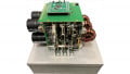
Sigma fxP PVD backside metallization system. Image Courtesy of SPTS.
Handling Thin Wafers
As the wafer gets thinner, the wafer bow becomes increasingly challenging. The wafer bow is a measure of the flatness of wafers. A wafer bow is generally caused by unequal stresses on the surface of the wafer. Therefore, manufacturers prefer silicon strengthening techniques such as the TAIKO thinning process, where a ring is left on the wafer's outer edge to reduce the risks of wafer breakage or edge clipping.
The main hardware requirement for the BSM PVD processing is that handling systems must support wafers at the very edge for TAIKO compatibility and can handle warped wafers, as TAIKO processing does not eliminate the problem of warping completely.
Moreover, as the wafers are processed upside down, the front side of the wafer mustn't be damaged through direct contact with chamber hardware.
To cater to all these needs of wafer handling, SPTS’s Sigma fxP offers an edge contact handling option where only the outer edge of the wafer is supported throughout its processing in the machine. This option combines with modified robot handling velocities to enable reliable handling and avoid any front side damage.
Removing Contaminants
In power devices, thick aluminum alloy or copper layers are deposited on the front side of the wafer to manage high currents. But this approach puts large heat loads on process chamber hardware, which can result in film contamination from outgassing chamber furniture. This contamination can lead to the formation of whiskers/extrusions in the film.
Organic-based materials such as Polyimide (PI) can absorb contaminants before deposition. For ultra-thin silicon cases, thorough degas are required to fully outgas the wafer. The multi-wafer degas (MWD) technology from SPTS overcomes all the challenges without compromising throughput. With this technology, manufacturers can deposit thick metal layers without any yield affecting whiskers or extrusions.

Multi-wafer degas (MWD). Image courtesy of SPTS.
Annealing
After metalized interconnections have been deposited and etched, annealing may be performed for optimization and stabilization of the devices. It involves combining hydrogen with uncommitted atoms at or near the silicon-silicon dioxide interface.
Conventional approaches rely on consistent, repeatable wafer scheduling and chamber pump recovery performance between wafers to ensure optimal wafer to wafer repeatability. The traditional techniques may also affect the throughput. The Sigma fxP performs the Al annealing on-site and in the Al deposition chamber itself, avoiding any scheduling or vacuum recovery concern.
Stress Control
After the Al layer, the remaining layers are deposited in low temperatures to minimize extrinsic stress and warpage. SPTS uses a backfill cool technique to remove heat from wafers as they arrive from previous heat processes. The technique involves increasing chamber pressure to a level that will conduct heat away from the wafer.

Backfill cool technique. Image Courtesy of SPTS.
In addition, pulsed DC, N2 addition, and traditional pressure adjustment can be used to tune the wafer bow accordingly.
For thin silicon mounted on carriers, cold 'electrostatic chuck (ESC)' technology is used to remove heat from wafers efficiently.
The backside metallization process presents many challenges and demands new and optimized processing technologies at each stage. Sigma fxp is meant for all those requirements, using edge contact processing, batch vacuum degas, low damage etch, and backfill processing to either put heat into wafers for ohmic contact or take the heat out for stress control/bow reduction, which is a relatively efficient approach to heat transfer that is compatible with fragile, thin wafers and proven in production.