Facebook
 Google
 GitHub
 Linkedin
100 V GaN Transistor for AI, Industrial, and Motor-Drive Applications
Learn how EPC’s 100 V EPC2375 GaN transistor features a novel 3-pad package that reduces resistance and maximizes efficiency, driving higher power density for AI, robotics, and industrial motor applications.
This article is published by EEPower as part of an exclusive digital content partnership with Bodo’s Power Systems.
Artificial intelligence (AI) computing, robotics, autonomous machines, and industrial automation are driving demand for smaller, more efficient power electronic converters. With conventional silicon (Si) MOSFETs, engineers have traditionally faced a trade-off between efficiency and power density, as the higher switching frequencies required to reduce converter size typically result in increased switching losses and lower overall efficiency.
Recent gallium nitride (GaN) products have largely eliminated this compromise by enabling both higher switching frequencies and higher efficiency [1]. As a result, power converters can achieve greater power density without sacrificing performance.
Today, 48 V systems are ubiquitous in AI server racks, humanoid robots, drones, automotive electronics, and industrial equipment. Consequently, 80 to 100 V-rated devices have become key building blocks in the power conversion systems present in these applications.

Image used courtesy of Freepik
EPC2375 Description
EPC2375 is EPC’s newest 100 V-rated GaN transistor. Like other parts from EPC such as EPC2361, it uses a 3 mm by 5 mm PQFN package with an exposed top for double-sided cooling. A distinguishing feature of EPC2375 is its new three-pad package, the first specifically optimized for GaN transistors.
As shown in Figure 1(a), the package incorporates large drain and source pads that maximize thermal conduction to the PCB while minimizing parasitic resistance. Combined with a 0.8 mm clearance between the drain and source terminals, this layout simplifies PCB routing and facilitates paralleling multiple devices in high-current applications such as motor drives, data-center DC-DC converters, synchronous rectifiers, resonant converters, and other hard- and soft-switched power converters.
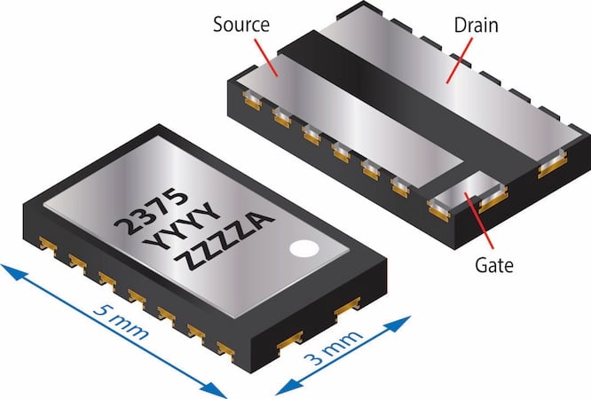
Figure 1. EPC2375 package and size. Image used courtesy of Bodo’s Power Systems [PDF]
Table 1. Comparison of key device parameters for various GaN devices.
|
Part Number |
VDS (V) |
RDS(on) (mΩ) |
QG (nC) |
Qoss (nC) |
QGD (nC) |
QRR (nC) |
Area (mm2) |
|
EPC2375 |
100 V |
0.9 |
19 |
78 |
2.3 |
0 |
15 (3-pad) |
|
GaN A |
100 V |
1.3 |
16 |
63 |
4.9 |
0 |
15 |
|
GaN B |
100 V |
2.2 |
14 |
85 |
3 |
0 |
15 |
|
Si A |
80 V |
2.3 (5 VGS) |
55 |
76 |
15 |
47 |
30 (3-pad) |
|
Si B |
80 V |
1.9 (6 VGS) |
75 |
133 |
25 |
71 |
30 (3-pad) |
|
Si C |
100 V |
3.15 (5 VGS) |
40 |
91 |
13 |
42 |
30 (3-pad) |
In addition to its new package, EPC2375 offers a typical RDS(on) of less than 1 mΩ while maintaining state-of-the-art switching characteristics. As summarized in Table 1, which compares EPC2375 with other GaN and Si devices in the same voltage class (80 V – 100 V), EPC2375 provides more than 40% lower on-resistance than the closest GaN competitor and less than one-quarter that of the closest silicon alternative for a comparable footprint.
Despite its exceptionally low RDS(on), EPC2375 also exhibits lower QOSS and QGD than competing GaN alternatives. This combination of low conduction and switching losses makes it particularly well suited for both hard-switched and resonant power converter topologies. Under these operating conditions, conventional Si MOSFETs cannot achieve a comparable balance of efficiency, switching performance, and power density.
EPC90189 - Evaluation Platform
To accelerate device evaluation and simplify converter development, EPC offers the EPC90189 evaluation board [2], a compact platform designed to demonstrate the capabilities of the EPC2375 eGaN FET. The board integrates two EPC2375 transistors in a half-bridge configuration together with a high-speed gate driver, a programmable dead-time generation circuit, input capacitors, Kelvin sense points, and high-current power connectors.
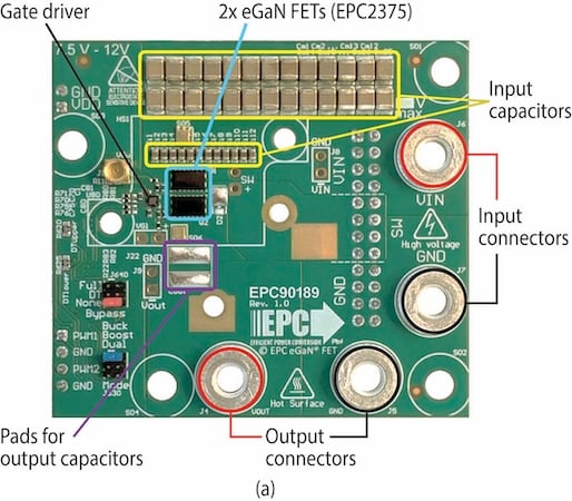
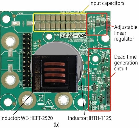
Figure 2. a) Top view of EPC90189 board; b) bottom view of EPC90189; c) EPC2375. Image used courtesy of Bodo’s Power Systems [PDF]
The board also provides footprints for output ceramic capacitors and a range of inductor packages, allowing engineers to configure it as either a buck or a boost converter. This flexibility enables rapid evaluation of EPC2375 under a wide variety of operating conditions without requiring a custom PCB design. In addition, EPC90189 is designed to facilitate accurate electrical characterization, with dedicated test points for high-quality measurements of the switch node, high-side, and low-side gate waveforms.
Figure 2 highlights the top and bottom sides of the evaluation board together with several key components. The bottom side includes a configurable linear regulator that supplies the gate driver and the dead-time generation circuit. The dead-time circuit allows the half-bridge to be driven from a single PWM input by generating a complementary gate signal with tightly controlled dead time.
Depending on the selected routing configuration, the PWM signal can be applied to either the high-side or low-side device, allowing the board to operate as a buck or boost converter, respectively. The board also supports multiple inductor footprints and accommodates an off-the-shelf heatsink for higher-power operation.
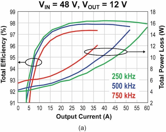
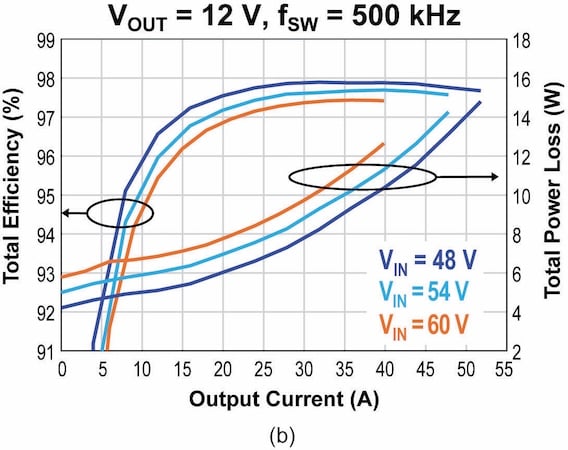
Figure 3. a) Performance of EPC90189 with various switching frequencies; b) Performance of EPC90189 with multiple input voltages. Image used courtesy of Bodo’s Power Systems [PDF]
EPC2375 Performance in EPC90189
The performance of EPC2375 was evaluated using the EPC90189 board configured as a synchronous buck converter under various input voltages and switching frequencies. Figure 3(a) presents the measured efficiency and power loss at switching frequencies ranging from 250 kHz to 750 kHz for a 48 V input and a regulated 12 V output.
Figure 3(b) shows the corresponding performance at a fixed switching frequency of 500 kHz with input voltages ranging from 48 V to 60 V. The same 2.2 µH inductor [3] was used for all tests, and the output current was increased until the device case temperature reached approximately 100°C. Measurements were performed with 400 LFM of forced airflow and without the use of a heatsink.
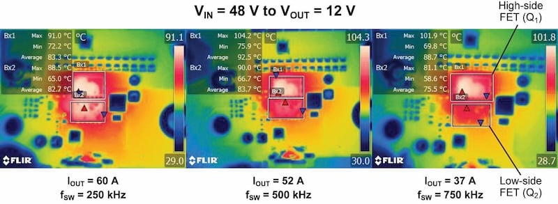
Figure 4. Thermal images of EPC90189 operated as a 48 V to 12 V synchronous buck converter at various switching frequencies. The board was cooled with 400 LFM of forced airflow and no heatsink. Images were captured in steady state. Image used courtesy of Bodo’s Power Systems [PDF]
The results demonstrate that EPC2375 maintains excellent efficiency over a broad range of operating conditions. For example, at 500 kHz, the board can deliver over 500 W into a 12 V load with full-load efficiency of nearly 98%. At 250 kHz, the output power can be increased to over 700 W while achieving the same full-load efficiency.
Figure 4 presents thermal images of the high-side and low-side transistors operating at different switching frequencies. At 750 kHz, the case temperature difference between Q1 and Q2 is approximately 20°C, whereas at 250 kHz this difference decreases to only about 3°C. This indicates a more balanced distribution of losses between the two devices at the lower switching frequency.
Board Layout
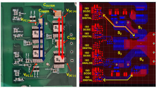
Achieving the performance demonstrated by EPC90189 requires careful PCB layout to minimize parasitic impedances (both resistance and inductance) [1]. To illustrate the design approach, Figure 5 presents key sections of the board layout.
On EPC90189, the EPC2375 devices and gate driver are located on the top side of the board. The high-frequency bypass capacitors are also located on the top layer, just above the high-side FET. The first inner layer (mid-layer 1) is used as a ground return to close the power loop, connecting the source of the low-side FET to the bypass capacitors. Together, these two layers define both the power and gate loops and therefore have the greatest influence on switching performance.
A key aspect of the layout is the relative orientation of the power loop (blue arrows) and the high-side and low-side gate loops (yellow and green arrows, respectively). They are arranged approximately perpendicular to one another to minimize common-source inductance and reduce coupling between the power and gate-drive paths.
Another important feature is the switch-node copper plane located beneath the high-side gate resistors, bootstrap capacitor, and high-side gate-driver pins. This plane provides both shielding and a low-impedance connection between the high-side transistor and the gate driver. Although overlap between the switch-node plane and adjacent VIN or ground planes is often viewed as undesirable, the resulting parasitic capacitance is at least two orders of magnitude smaller than the transistor output capacitance (QOSS).
Consequently, its impact on switching performance is negligible. The same design philosophy applies to the low-side gate-drive loop, although its implementation is generally simpler because the first internal layer already provides a continuous ground plane.
Via placement is equally critical in high-current, multilayer PCB designs. A large number of vias is recommended to distribute current evenly among all layers. At the same time, it is important to preserve a low-impedance ground return in the first internal layer. In EPC90189, this objective is achieved by staggering the switch-node and VIN vias, leaving sufficient copper between adjacent vias to maintain a continuous, low-impedance ground path.
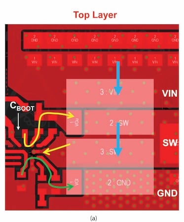
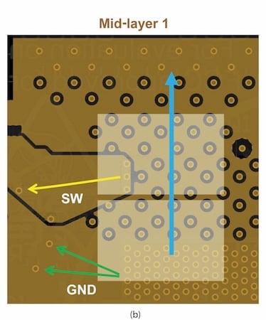
Figure 5. Layout of EPC90189 with the EPC2375 FETs highlighted and the power and gate loops indicated with arrows: a) top layer; b) mid-layer 1. Image used courtesy of Bodo’s Power Systems [PDF]
Conclusions
EPC2375 extends the performance of 100 V GaN technology by combining an innovative package with industry-leading electrical characteristics. Its three-pad package reduces parasitic resistance, improves thermal performance, and simplifies PCB layout, making it particularly well suited for high-current applications where both electrical and thermal performance are critical.
The experimental results obtained using the EPC90189 evaluation board demonstrate that a single-phase buck converter using EPC2375 can deliver over 700 W to a 12 V load from a 48 V input, while maintaining a full-load efficiency of 98%.
Moreover, this performance is achieved without a heatsink and with only 400 LFM of airflow. The evaluation results also highlight the importance of careful PCB layout when designing high-performance GaN converters. Minimizing parasitic impedances is essential for achieving clean switching waveforms, high efficiency, and balanced thermal performance.
As power systems continue to demand higher power density and efficiency, innovations in both device packaging and PCB layout will play an increasingly important role in enabling the next generation of high-performance GaN power converters.
References
[1] A. Lidow, M. De Rooij, J. Glaser, A. Pozo, S. Zhang, M. Palma, D. Reusch, and J. Strydom, “GaN Transistors for Efficient Power Conversion,” 4th ed. John Wiley & Sons, 2025. ISBN: 978-1394286959.
[2] Efficient Power Conversion, “EPC90189: 100 V, 60 A GaN-based Half-bridge Evaluation board”
[3] Wurth Elektronik, “74437625200222 Datasheet WE-HCFT Flat THT High Current Inductor”
This article originally appeared in Bodo’s Power Systems [PDF] magazine.
Related Content