Facebook
 Google
 GitHub
 Linkedin
Researchers Explore Carbon Impurities in Gallium Nitride Semiconductors
Scientists from the Nagoya Institute of Technology (NITech) have conducted innovative research about the role of impurities in Gallium Nitride (GaN) semiconductors and how to mitigate their effects.
According to the team led by Professor Masashi Kato, the new findings could lead to lower power losses in electronic devices and consequent energy savings. The study was recently published in the Journal of Applied Physics.
Gallium Nitride Semiconductors: an Overview
Silicon-based MOSFETs (Metal Oxide Semiconductor Field Effect Transistors) have been used since the early days of electronics to convert energy to power.
However, the increasing specifications of recent electronics are making silicon MOSFETs reaching their limits, particularly when it comes to power density and efficiency requirements.

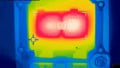
Carbon impurities in gallium nitride (GaN) semiconductors can degrade performance. Image used courtesy of Nagoya Institute of Technology.
In addition, silicon is also an environmentally polluting material, and due to greener regulations adopted by companies around the world, many governments are trying to find more sustainable alternatives.
Gallium nitride is one such material, offering a relatively larger bandgap than silicon, which in turn allows for more efficient high-voltage and high-temperature applications.
It also is environmentally more sustainable and ensures fewer switching losses during switching applications thanks to the fact that current travels quicker through GaN than through silicon.
Impurities’ Effects in Gallium Nitride Semiconductors
While desirable over traditional silicon, however, GaN semiconductors are subject to impurities such as carbon atoms that can lead to poorer switching performance, the new research claimed.
The trapping of charge carriers in ‘deep levels’ - created by the impurity defects in the GaN crystal layers - is believed to originate from the presence of a carbon impurity on a nitrogen site.
"Only after understanding the impacts of impurities in GaN power semiconductor devices can we push for the development of impurity control technologies in GaN crystal growth," Kato said, commenting on the study’s publication.
To understand the impact of such impurities, Kato’s team prepared two samples of GaN layers grown on GaN substrates, one doped with silicon and the other with iron.
What they noticed as part of the experiment was that during the silicon doping process using a 1 nanosecond-long UV laser pulse, unintentional doping of carbon impurities happened.
In both samples, however, the decay time declined above 200°C.
Kato said the findings can be explained by looking at the deep levels as trapping "holes" (absence of electrons). Eventually, they get recombined with free electrons but the time to do so is not sufficient to allow an electron to be captured by the deep level.
At high temperatures, however, the holes managed to escape from the trap and be recombined with the electrons through a quicker recombination channel.

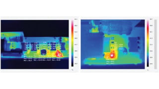
An analytical model explaining the new findings. Image used courtesy of Nagoya Institute of Technology.
"To reduce the effects of the slow decay component, we must either maintain a low carbon concentration or adopt device structures with suppressed hole injections," Kato explained.
The Nagoya Institute of Technology
Founded in 1905 as Nagoya Higher Technical School, the educational institution was refounded in 2004 with its current name.
Today, NITech comprises the Faculty of Engineering, the Graduate School of Engineering, and four Educational Research Centers.
Dr. Masashi Kato is an associate professor at the Department of Electric & Mechanical Engineering at NITech.
His research focuses on semiconductor characterization, power devices, artificial photosynthesis, and integrated circuits.
According to Kato, the latest findings about impurities in GaN semiconductors could pave the way for greener electronics applications.
"GaN enables lower power losses in electronic devices and therefore saves energy,” he explained, “I think it can go a long way in mitigating greenhouse effects and climate change."