Facebook
 Google
 GitHub
 Linkedin
Gallium Nitride Discovery Aims for Efficient P-Type GaN Transistors
Gallium nitride, a semiconductor that revolutionized energy-efficient LED lighting, could also transform electronics and wireless communication, thanks to a discovery made by Cornell researchers.
Their paper, "A Polarization-Induced 2D Hole Gas in Undoped Gallium Nitride Quantum Wells," was published Sept. 26 in Science.
Silicon has long been the king of semiconductors, but it has had a little help. The pure material is often augmented, or "doped," with impurities like phosphorus or boron to enhance current flow by providing negative charges (electrons) or positive charges ("holes," the absence of electrons) as needed.
In recent years, a newer, sturdier family of lab-grown compound semiconductor materials has emerged: group III-nitrides. Gallium nitride (GaN) and aluminum nitride (AlN) and their alloys have a wider bandgap, allowing them to withstand greater voltages and higher frequencies for faster, more efficient energy transmission.
"Silicon is very good at switching off and on and controlling electrical energy flow, but when you take it to high voltages it doesn't operate very well because silicon has a weak electric strength, whereas GaN can sustain much higher electric fields," said co-senior author Debdeep Jena, the David E. Burr Professor in Electrical and Computer Engineering and in Materials Science and Engineering. "If you're doing very large amounts of energy conversion, then wide-bandgap semiconductors such as GaN and silicon carbide are the solutions."
Since the 1990s, researchers have doped GaN by adding magnesium impurities to create holes, but the process is highly inefficient. For every hundred magnesium atoms introduced into the crystal, only three or four holes might appear at room temperature, and even fewer at low temperatures.
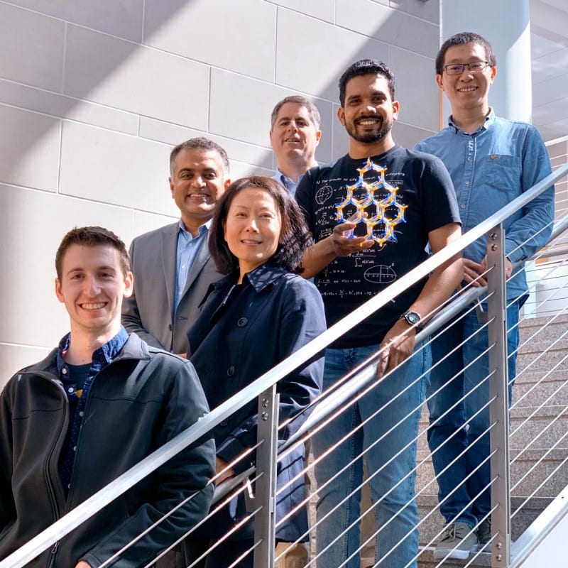 From left, Ph.D. student Samuel J. Bader; Debdeep Jena, professor of electrical and computer engineering and materials science and engineering; Huili Grace Xing, professor of electrical and computer engineering and materials science and engineering; David Muller, professor of applied and engineering physics; Ph.D. student Reet Chaudhuri; and postdoctoral associate Zhen Chen have discovered fast-moving positive charges in gallium nitride that could transform electronics and wireless communication. (image credit, Jimy Encomendero)
Rather than using impurities, Ph.D. student Reet Chaudhuri stacked a thin GaN crystal layer - called a quantum well - atop an AlN crystal, and the difference in their crystal structures was found to generate a high density of mobile holes. Compared with magnesium-doping, the researchers discovered that the resulting 2D hole gas makes the GaN structures almost 10 times more conductive.
"In 1992, researchers discovered that when aluminum nitride is deposited on top of gallium nitride, you get free electrons at the interface. Having electrons conduct inside GaN makes what we call n-type electronic devices," said Chaudhuri, the paper's lead author. "The polarization theory that explains why we get mobile electrons in this structure, which in fact was conceptualized and validated by Cornell researchers in late '90s, also predicts that we should expect holes when the structure is flipped. But to date, there had not been any report of holes in an undoped III-nitride semiconductor structure. And that's what we have found in this work."
Using the new material structure created by Reet, co-author and Ph.D. student Samuel James Baderrecently demonstrated some of the most efficient p-type GaN transistors in a collaborative project with Intel. Now that the team has the capability to make hole-channel transistors - which are called p-type - they plan to pair them with n-type transistors to form more complex circuits, opening up new possibilities in high-power switching, 5G cellular technology and energy efficient electronics, including phone and laptop chargers.
"It's very difficult to simultaneously achieve n-type and p-type in a wide bandgap semiconductor. Right now, silicon carbide is the only other one that has both besides GaN. But the mobile electrons in silicon carbide are more sluggish than those in GaN," said co-senior author Huili Grace Xing, the William L. Quackenbush Professor in electrical and computer engineering and in materials science and engineering. "Using these complementary operations enabled by both n-type and p-type devices, much more energy efficient architecture can be built."
Another advantage of the 2D hole gas is that its conductivity improves as the temperature is lowered, meaning that researchers will now be able to study fundamental GaN properties in ways that haven't been previously possible. Equally important is its ability to retain energy that would otherwise be lost in less efficient power systems.
"Gallium nitride caused a revolution in the lighting industry," Jena said. "It enabled the white lighting that is in our cellphones, laptops, and LED bulbs that are replacing the incandescent bulbs in our homes. With a regular 100W incandescent light bulb, which is about 4% energy efficient, you might get 4 watts of light and the rest is heat. You know this very well if you touch the bulb when it is on. LEDs on the other hand can be almost 80% efficient, and only 20% is heat. A similar change in energy-efficiency of electronics has not yet happened. And maybe this finding is a step in that direction."
A patent application has been filed through the Center for Technology Licensing for the discovery. Other contributors included David Muller, the Samuel B. Eckert Professor in Applied and Engineering physics; and Zhen Chen, a postdoctoral researcher in Muller's lab.
The research was supported in part by Intel, the Air Force Office of Scientific Research, the National Science Foundation and the Cornell Center for Materials Research.
Related Content