Facebook
 Google
 GitHub
 Linkedin
Atomera to Discuss Semiconductor Materials Advancements
Atomera Incorporated will be holding meetings with customers, analysts, media and investors during the 2017 Consumer Electronics Show (CES) January 5-7, 2017 in Las Vegas at the Bellagio Hotel. Atomera's Mears Silicon Technology (MST®) is currently being evaluated by foundries and integrated device manufacturers.
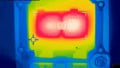
Mears Silicon Technology™ (MST®) is a patented, quantum engineered material which enhances transistors to deliver significantly better performance in today's electronics. That means consumer electronics, such as mobile phones will have longer battery life, IOT devices can be made smaller, and cloud computing will become even more powerful.
Atomera will be sharing its semiconductor materials innovations, which are focused on extending the life of Moore's Law, including discussing: Quantum engineered materials -- The future of semiconductors will be dominated by "More-than-Moore" architectural and material innovations. Atomera's MST® technology delivers those advancements today.
Making electronics faster and more efficient -- By combining a materials breakthrough with other patented techniques, Atomera enables more efficient and better controlled current flow, leading to dramatic improvements in device performance and power efficiency.
How Atomera breathes new life into semiconductor fabs -- MST squeezes up to a full node of benefits out of fab processes. With an MST license, manufacturers can address their yield, power and performance challenges at a fraction of the cost of alternative approaches.
Atomera has developed Mears Silicon Technology™ (MST®), which increases performance and power efficiency in semiconductor transistors. MST® can be implemented using equipment already deployed in semiconductor manufacturing facilities and is complementary to other nano-scaling technologies already in the semiconductor industry roadmap.