Facebook
 Google
 GitHub
 Linkedin
3D Printing of Electrically Shielded Conductive Traces
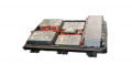
Nano Dimension Ltd.announced today that Nano Dimension Technologies, a fully owned subsidiary of Nano Dimension, has developed the technology for the printing of shielded conductors combined in a printed circuit board (PCB). The patent presents an innovative solution for the phenomenon of electric power loss in PCBs that are primarily used in the communication industry.
The communications industry requires high speed data transfer, where current high speed circuitry reaches speeds of 60G-100G. PCBs for this industry suffer from losses between the conductive traces (CROSSTALKS) and other phenomena arising from the multiplicity of signals. The loss phenomenon interferes with the proper function of the electric circuit and can prevent its proper function.
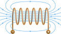
Nano Dimension has developed a unique 3D printing method that creates printed sheaths to shield the conductors like a form of insulated cable, and this new printing method allows the sheaths to be built into the PCB object. This innovative approach creates the opportunity to minimize the size of PCBs used in the high speed communication space.
By selectively depositing Nano Dimension's conductive ink, one can build a shield along the entire length of the conductor at a minimal distance. This prevents leakage and loss and is similar to the current practice of using shielded cables with the PCB externally. 3D printing allows the shielded cables to be embedded.