Facebook
 Google
 GitHub
 Linkedin
Toshiba’s 40 Volt, Low-Spike-Type Power MOSFET Aims to Reduce EMI
The N-Channel device’s low-spike capability serves to diminish overshoot in power switching applications.
The TPHR7404PU employs Toshiba’s latest generation U-MOSIX-H process.

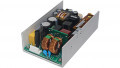
The TPHR7404PU. Image courtesy of Toshiba
The TPHR7404PU features a cell structure utilizing a parasitic snubber, lowering voltage peaks, effectively reducing the noise and ringing inherent to high speed switching. With a VGS of 10 volts, maximum RDS(ON) is 0.74mΩ. The problems associated with unintended turn on are avoided due to the MOSFET’s gate threshold voltage, which ranges from 2 to 3 volts (ID = 1 mA)
Toshiba’s Low Spike Technology
Specific details for the U-MOSIX-H process are scarce, but this isn’t Toshiba’s first effort in this arena. A glimpse at the structures of U-MOSVIII-H and IX-H generations will be revealing.
Due to the nature of the process, parasitic resistances and capacitances are inevitably introduced between the drain and the source, as illustrated in the diagram below.

A MOSFET parasitic snubber circuit. Image courtesy of Toshiba
The resistance and capacitance combine to form a classic RC snubber circuit, again as illustrated in the diagram. This snubber will, of course, serve well to reduce spikes, aka overshoots, to the benefit of designers.
Standout Features
-
Channel-to-case thermal resistance is 0.71°C/W
-
Switching gate charge (QSW) is 34 nC (typical)
-
Output charge (QOSS) is 90 nC (typical)
-
Leakage current (IDSS) is 10 μA (max) with VDS at 40 volts
Absolute Maximums
These ratings are generally taken at 25℃. They may be subject to conditions enumerated in the datasheet.
-
Drain-source voltage is 40 volts
-
Gate-source voltage is ±20 volts
-
Drain current is 150 amps
-
Drain current, pulsed (t = 100 μs) is 500 amps
-
Power dissipation is 210 watts
-
Single-pulse avalanche energy is 298 mJ
-
Channel temperature is 175 ℃
Thermal Characteristics
These are maximum values:
-
Channel-to-case thermal resistance is 0.71 ℃/W
-
Channel-to-ambient thermal resistance 50 ℃/W
-
Channel-to-ambient thermal resistance 156 ℃/W
Static Electrical Conditions
-
Gate leakage current is ±0.1 µA (max)
-
Drain cut-off current is 10 µA (max)
-
Drain-source breakdown voltage is a minimum of 40 or 25 volts, depending of on gate-source voltage
-
Drain-source breakdown voltage is 25 volts, minimum
Dynamic Electrical Characteristics
The specifications below are typical values:
-
Input capacitance is 6960pF
-
Reverse transfer capacitance is 130pF
-
Output capacitance is 2060pF
-
Gate resistance is 3Ω
Gate Charge Characteristics
The characteristics cited here are typical values:
-
Total gate charge (gate-source plus gate-drain) is 98 or 62 nC, depending on gate-source voltage
-
Gate-drain charge is 18 nC
-
Gate switch charge is 34 nC
-
Output charge is 90 nC
Applications
-
High-efficiency DC-DC converters
-
Motor drivers
-
Switching voltage regulators
Physical
-
The TPHR7404PU is available in a 5 x 6 mm SOP advance package
Regulatory and Safety
- Toshiba recommends that designers and OEMs contact a sales representative about RoHS compatibility