 Facebook
 Google
 GitHub
 Linkedin
Nexperia Debuts Tiny 20 V and 30 V MOSFETs in DFN Packages
The company says its fresh DFN MOSFETs, which measure 0.63 x 0.33 x 0.25 mm, are the world’s smallest.
At a full 13% smaller than devices offered in the next smallest DFN0604 package, Nexperia says its latest DFN0603-packaged MOSFETs, released last Wednesday, save designers crucial board space with no compromise in performance.

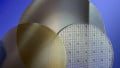
Nexperia says its new MOSFETs take up 13% less space than previous devices. Image used courtesy of Nexperia
The fresh four-member trench MOSFET family sports a 74% reduction in RDS(ON)s, the company says, when compared to devices ensconced in DFN0604. Included is one 20 V and one 30 V N-channel device, a 20 V N-channel unit with 2 kilovolts (kV) of ESD protection, and a 20 V P-channel offering.
Each is available in surface-mounted, leadless packages. Nexperia plans to expand the range with two additional devices later this year.
Every 0.1 Millimeter Counts
Every tenth of a millimeter counts.
So said Sandy Wang, Nexperia’s product marketing manager for small-signal MOSFETs, in her recent post to the company’s blog.
Indeed, the difference between 0.24 and 0.20 square millimeters may seem trivially small. But this doesn't hold when considering items as small as earbuds, with their acute lack of available “board space,” if we can even call it that. Here, saving every 0.1 millimeter is vital.
Defining Terms
We have introduced the terms “RDS(ON)”, “Trench MOSFET,” and “P-channel” and N-channel” devices, so before we delve into specifics, let’s zero in on what these ubiquitous terms mean:
RDS(ON)
When a MOSFET is turned on, conduction is through the drain-source (d-s) pathway, and RDS(ON) stands for the resistance from drain to source. A low RDS(ON) value results in less energy being wasted in the MOSFET, and a corresponding reduction in parasitic heat generation.
P-channel and N-channel
In a low-side arrangement, the MOSFET electrically connects a load to ground, whereas a high-side design uses the MOSFET to connect the other end of the load to power. N-channel MOSFETS are used on the low side, and P-channel devices are used on the high side.
It should be noted, though, that N-channel devices can in fact be used on the high side, and engineers often elect to take the difficult steps in design necessary to do so thanks to these devices’ better overall specifications.
Trench MOSFETs
Classic MOSFETs are horizontally oriented devices, while Trench MOSFETs consist of vertical “trenches” that contain the gate dielectric. These trenches cut across the oppositely doped regions of the chip, as illustrated below.

A schematic of a trench gate power MOSFET. Image used courtesy of Nova Science Publishers, via arXiv
The trenches are connected in parallel, thereby greatly reducing the semiconductor’s RDS(ON).
The PMX100UN and the PMX100UNE
Both of these semiconductors are 20 V, N-Channel Trench MOSFETS. The defining difference between the two is that the latter sports 2 kV of human body model (HBM) ESD protection.

Schematic representations of the PMX100UN (left) and the PMX100UNE. Image [modified] used courtesy of Nexperia
Naturally, the devices sport similar specifications. Typical RDS(ON)s are 122 and 130 milliohms for the PMX100UN and the PMX100UNE, respectively. The former can handle 1.3 A across the d-s pathway when it is turned on to conduct current, while the latter is rated at 1.4 A.
The PMX300UNE
The PMX300UNE is a 30 V, N-channel Trench MOSFET.
It too features 2 kV of HBM ESD protection. Its typical RDS(ON) is 190 milliohms, with a maximum drain current of 820 milliamps. As an N-channel device, it is most typically employed in low-side load switching, as are the PMX100UN and the PMX100UNE.
PMX400UP
The PMX400UP is a 20 V, P-channel Trench MOSFET. As a P-channel semiconductor, it is more typically employed as a high-side load switch.
Typical RDS(ON) is 334 milliohms, and maximum drain current is specced at -900 milliamps.
Applications
These new semiconductors target battery switching, in addition to use as high-speed line drivers or as high-side or low-side load switches.
Physical Considerations
These devices operate over a -55 to 150 °C operating range.


Well Explained!!!