Facebook
 Google
 GitHub
 Linkedin
Infineon Introduces 650V High-Side And Low-Side Gate Drivers
The monolithic level-shift drivers include integrated bootstrap diodes to save space and reduce overall BOM.
The 2ED2110S06M and the 2ED210XS06F are the newest members of Infineon’s EICEDriver family. The units are based on the company’s silicon-on-insulator technology, with each transistor isolated by buried silicon dioxide, preventing parasitic latch over all temperature and voltage conditions.

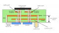
The 2ED2110S06M. Image courtesy of Infineon’s Datasheet
The newest EICEDrivers are designed to drive MOSFETs and IGBTs. They feature operating voltages of up to +650 volts and negative VS transient immunity of 100 volts. They offer UVLO for both channels and Schmitt trigger inputs with hysteresis. Maximum supply voltage is 25 volts, and the units are compatible with 3, 5 and 15 volt input logic. The gate drivers both feature a propagation delay of 90ns with a maximum of 10ns delay matching.
High Side Gate Drivers
In a previous article on the EICEDrivers, we illustrated a P-channel high side driver.

Image courtesy of EEPower
The problem here is that N-channel MOSFETs have superior RDS(ON)s as compared to P-channel devices. In order to use an N-channel MOSFET as a high side driver, a Bootstrap diode is necessary.
What is a Bootstrap Diode?
In the image below, an N-channel device is proposed as a high side gate driver.

N-channel MOSFET as a high side driver. Image courtesy of MOSFET Bootstrapping video (4:10)
But, a 12-volt input signal to the gate will not sustain current across the load. That’s because with 12 volts across the load, the source is also at 12 volts, and there will be no potential difference between gate and source. To provide a differential of 12 volts between gate and source, 24 volts is needed at the gate.
To generate the extra voltage, a bootstrapping circuit is devised, composed mainly of a capacitor and the bootstrap diode. The diode charges the capacitor up to the power supply voltage, and at the right moment, that power supply voltage is added to the 12-volt input signal, enough to turn on the MOSFET and power the load. A lengthy description of the circuitry and of calculating the size of the capacitor is provided in section 5.8 of the 2ED2110S06M datasheet
The 2ED2101S06F
The 2ED2101S06F provides 0.29 and 0.7 amps of source and sink current, respectively.

A typical, but simplified illustration of the 2ED2101S06F driving two N-channel MOSFETS. Image courtesy of datasheet
Note that the RBS, in series with the bootstrap diode, serves to prevent high inrush current when charging the bootstrap capacitor.
Applications for the 2ED2101S06F include:
- EV charging stations and battery management
- Robotics
- Servo motors
- SMPS power management, a reference design is provided
- Smart buildings
- LED lighting
The 2ED2110S06M
This driver typically provides 2.5 amps source and sink current.
Applications for the 2ED2110S06M include:
- Industrial welding and heating
- Motor drives and control
- Power tools
- Smart building
- Solar power energy systems
Physical
- The 2ED2119S06M is available in a 10.65 x 10.5 mm DSO-16 package
- The three 2ED210XS06F versions come in 6 x 4.9 mm DSO-8 packages
- The recommended operating temperature range of both devices is from -40 to +125℃
Environmental
- Both units are RoHS compliant