Facebook
 Google
 GitHub
 Linkedin
GaN Chip Saves Space, Costs in Battery Management Systems
Innoscience is expanding its family of VGaN products with a device rated to 100 V capable of significantly reducing the solution size for 48 V and 60 V battery management systems.
Innoscience Technology has released the INV100FQ030A, a 100 V, bidirectional extension to its low-voltage family of VGaN power ICs. The chip extends the voltage capabilities of the product family, making it an ideal solution for high-frequency 48 V and 60 V battery management systems (BMS).
With its higher voltage rating, the INV100FQ030A replaces back-to-back silicon MOSFET configurations, reducing the size of the typical battery charge/discharge management circuit by up to one-third.
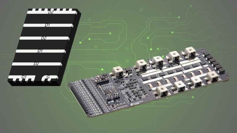
The INV100FQ030A. Image used courtesy of Innoscience
The devices are well-suited to BMS circuits used in mid-sized battery-powered devices like home batteries, e-bikes, and portable charging stations. In addition to BMS applications, the INV100FQ030A can be used as a high-side load switch in converters and other power-switching applications.
GaN-on-SiC Device Technology
Innoscience is one of the world’s largest integrated device manufacturers using 8-inch wafers to develop gallium nitride (GaN) solutions. The company designs its GaN devices for a wide range of applications accommodating voltages ranging from 30 V to 650 V.
Most GaN HEMT (high electron mobility transistors) devices are naturally depletion-mode (d-mode) and operate normally-on. A normally-on state means the device conducts current when no gate voltage is present. This is contrary to industry norms for normally-off devices and typically necessitates specialized drive circuitry.
Innoscience’s GaN-on-Silicon technology allows it to develop intrinsically normally-off, or enhancement mode (e-mode), GaN HEMTs. Normally-off operation is developed using p-GaN materials layered on top of the AlGaN barrier, which, combined with the gate metal, modifies the potential in the channel to yield a normally-off state.

Normally-off GaN-on Silicon device technology. Image used courtesy of Innoscience
Space Reduction in Battery Management Applications
The first Innoscience VGaN device models were rated to 40 V and widely adopted in space-constrained mobile phone USB OVP (overvoltage protection) applications. In battery-powered systems, the OVP circuit protects the charging system from high input voltage conditions that could damage downstream circuitry.
With a 100 V rating, the device can be used in higher voltage (48 V and 60 V) systems like home batteries, portable charging stations, and e-bikes. For these higher voltage applications, two silicon MOSFETs are often used in series to meet voltage withstand requirements. With the INV100FQ030A, a single chip replaces both MOSFETs, resulting in up to 33% smaller and less expensive BMS solution.

Reducing BMS solution size. Image used courtesy of Innoscience (email)
With a low on-resistance of 3.2 mΩ, the INV100FQ030A is designed to perform its protective function with minimal impact on overall system efficiency. Bidirectional operation allows the GaN HEMT to support both charge and discharge cycles with two-way pass-through and two-way cutoff.
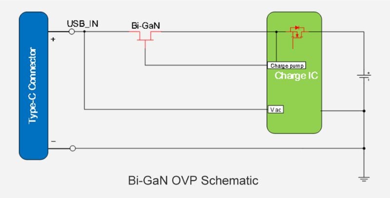
Battery management OVP circuit. Image used courtesy of Innoscience
Lowering the Cost of GaN
Cost remains a challenge for GaN products. Many GaN production facilities use 6-inch wafers in their device fabs, but by using 8-inch wafers for production, Innoscience can produce 80% more devices per wafer than conventional 6-inch wafers. The result is lower chip costs. Innoscience has also equipped its production fabs with high-throughput silicon manufacturing tools optimized for speed and accuracy over the past 40 years.
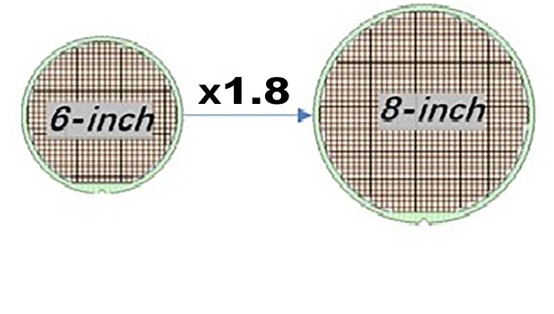
8-inch wafers yield 80% more devices. Image used courtesy of Innoscience
By using a silicon-compatible manufacturing process, Innoscience intends to deliver more cost-competitive GaN solutions.