Facebook
 Google
 GitHub
 Linkedin
Utilizing the Programmable Ramp Generator on 8bit PICMCUs with MPLAB
The Programmable Ramp Generator (PRG), featured on several recent 8-bit PIC microcontrollers from Microchip Technology, is a highly flexible analog peripheral
The Programmable Ramp Generator (PRG), featured on several recent 8-bit PIC microcontrollers from Microchip Technology, is a highly flexible analog peripheral that is intended to simplify applications that require a linear change in voltage.
As its name implies, the PRG is able to produce rising, falling or alternating rising/falling ramps on its output under the control of software. However, once configured, the peripheral is able to operate independent of the core, freeing up the Central Processing Unit (CPU) to work on some other task, enter a lower power mode or otherwise take on a more supervisory role in the system. Rise and fall times can be adjusted dynamically by controlling an integrated constant current source. Flexible input and output options offer the designer freedom to interconnect with off-chip signal sources or with signals from other peripherals on the microcontroller. This often provides a more responsive system while minimizing potential noise sources and application size by reducing external component count. Figure 1 shows a block diagram of the peripheral.

Figure 1: Simplified PRG module block diagram
A useful tool for configuring the PRG is the MPLAB Code Configurator (MCC), a user-friendly plug-in for the MPLAB X Integrated Development Environment (IDE) (see Figure 3). It generates drivers for controlling and driving peripherals of Microchip PIC microcontrollers such as the PRG. Different functions can be implemented with the PRG and each can be set up using MCC.

Figure 2: MCC – PRG module hardware settings
Triangular Wave Generator
A triangular wave generator (TWG) produces a periodic, non-sinusoidal waveform with a triangular shape of equal rise and fall times. To produce a triangular wave, the PRG must be configured in an alternating rising and falling mode. The MCC allows the configuration of the Rising (RS) and Falling (FS) timing input sources. The PRG determines the output oscillation frequency using these two voltage references that trigger the rise and fall of the ramp. These references also determine the minimum and maximum voltage peaks of the triangular wave signal.
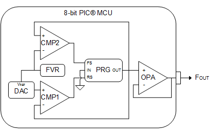
Figure 3: Peripheral integration for a Triangular wave generator
When the PRG output is below the voltage level set by a digital-to-analog converter (DAC), the RS input of the PRG is triggered and the internal capacitor is charged by the current source. When the PRG output exceeds the fixed voltage reference (FVR), the FS input is triggered and the internal capacitor is charged by the current sink.
Since the PRG does not have a designated output pin, the output of the PRG is buffered through a unity gain configured op amp. The output frequency can be calculated, but its accuracy may be affected by different factors such as the parasitic resistance of the capacitor, noise, production variance and temperature.
The value of the frequency varies by changing the output level of the DAC or the PRG’s slope rate (SR). The SR of the output ramp is configured through the PRG’s current settings.
Figure 4 shows the ideal behavior of the implementation. In general, the generated triangular wave consists of periodic and symmetrical alternating rising and falling ramps.

Figure 4: Triangular wave generator timing diagram
The maximum and minimum voltages are defined by VFVR and VDAC, respectively. The rise and fall triggers are set when the signal reaches either maximum or minimum voltage. Changing the slope rate setting in the MCC can be used to adjust the frequency. A change in VDAC also results to a change in frequency, but the minimum voltage will increase or decrease accordingly.
The oscillation frequency of the PRG depends on the selected current sink and source, the internal capacitance and the set rising and falling triggers. By placing additional capacitance on the output of the PRG, lower frequency ranges can be achieved.
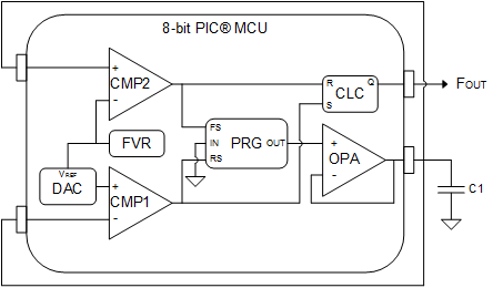
Figure 5: Adding CLC and a capacitor for lower frequency outputs
With an added Configurable Logic Cell (CLC) and external capacitor C1, the voltage trip points set by the DAC and the FVR can trigger the rising and falling events, respectively. C1 is added at the output of the op amp and effectively in parallel with the PRG’s internal capacitor. The additional capacitance drags out the time between trigger events, producing a lower frequency for FOUT.
Connecting the CLC at the output of the comparators lets the wave generator produce square waves and pulses. The CLC is configured as an SR latch and the low frequency FOUT is taken from its output. Similar to the PRG, the voltage references trigger the set and reset inputs. FOUT is set when the voltage at C1 (OPAOUT) falls below the DAC voltage level. Once OPAOUT rises above the FVR, FOUT is cleared.
Voltage-Controlled Oscillator
A voltage-controlled oscillator (VCO) is an electronic oscillator in which an input control voltage determines its frequency of oscillation. The instantaneous frequency of the VCO is usually designed to be in linear proportion with the instantaneous voltage; the higher the input voltage, the greater its oscillation frequency. The PRG’s operation for the VCO implementation is similar to the TWG, except the output frequency is taken from the CLC’s slope rate latch and a variable voltage VCNTRL sets the RS input of the PRG.
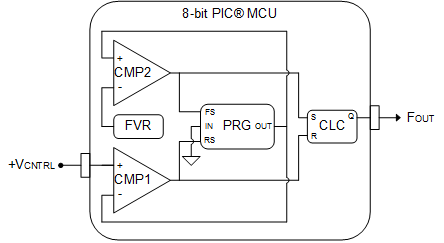
Figure 6: Configurations for a Voltage-controlled oscillator
A higher input for VCNTRL decreases the time needed to retrigger the rising event. Consequently, the switching between the current source and sink becomes faster and the oscillation frequency increases.
The relationship between the control voltage and output frequency is shown in figure 7 with three PRG slope rate values. The SR value can be varied for a desired range of frequencies. Lower SR values can produce frequencies ranging from a few hertz to around 500 kHz. Larger SR values, however, can reach up to the megahertz range.

Figure 7: VCO output frequency versus control voltage
With two control voltage values and a constant slope rate, a decrease in VCNTRL reduces the VCO frequency out of the CLC.
Voltage-Controlled Duty Cycle Oscillator
A standard VCO circuit directly modifies the oscillator frequency. For a Voltage-Controlled Duty Cycle Oscillator (VCDCO), its control voltage modifies the duty cycle of the output pulses.
A similar set-up to the VCO is implemented for the VCDCO with the exception that a time base triggers the start of the output pulse. The PWM and TMR modules determine the period and frequency of the oscillator while the PRG through VCNTRL determines its duty cycle.
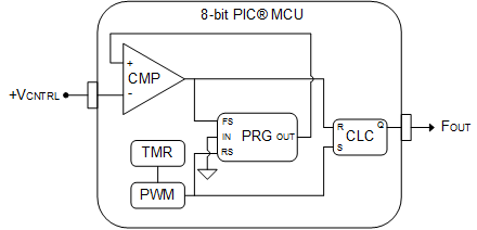
Figure 8: Using a time-based trigger for a voltage-controlled duty cycle
The rising edge of the PWM triggers the PRG RS input and sets the CLC. When the PRG output exceeds VCNTRL, the FS input is triggered, the PRG capacitor is shorted and the CLC is reset. The PRG and CLC output will remain low until the next TMR overflow and PWM positive edge.
Increasing VCNTRL prolongs the rise of the ramp and the output’s positive pulse width.
The duty cycle is computed as a ratio of VCNTRL to VMAX. To increase the range of duty cycles, the timer period should be equal to the rise time of the ramp when it reaches VMAX with the given slope rate.
When two different values of VCNTRL are used, the RS trigger sequence can be uniform in both conditions due to the constant period of the timer and PWM. However, there can be an additional delay before the FS trigger due to the constant slope rate and higher VCNTRL.
The PRG slope rate and TMR2 period values depend on the required frequency and duty cycle range of the VCDCO. The duty cycle of the PWM can be set low enough to trigger the RS input of the PRG. FOUT is still taken from a CLC SR latch. The PWM and CMP outputs also provide the set and reset inputs for the CLC.
Asynchronous One-Shot
An asynchronous one-shot (AOS) produces a single-output pulse when it is triggered externally. Commonly known as monostable multi-vibrators, the AOS has one stable state. If its stable state is low, an external trigger drives the output high for a specific period. At the end of one period, the AOS returns to its stable state and will wait for the next trigger event.
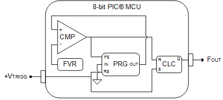
Figure 9: Using an external trigger for one-shots
The reset state of the CLC is the stable state of the AOS. An external trigger sets the RS input of the PRG and sets the output of the AOS out of the CLC. When the PRG reaches the FVR, the FS input source is triggered, the internal capacitor in the PRG is shorted and the CLC output is reset. The duration of the pulse width depends on the FVR voltage and PRG slope rate.
An external voltage trigger can replace the PWM and TMR modules to remove the periodic trigger sequence of the PRG RS input and CLC set sources. The output pulses are taken from the CLC output.
Voltage-Controlled One-Shot
This next example is an upgrade of the previous one-shot. One input acts as a trigger, while an additional input determines the one-shot period. One application of the one-shot controls the on-time of a Critical Conduction Mode (CrCM) PFC controller.
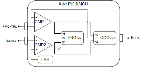
Figure 10: Configurations for a voltage-controlled one-shot
The input voltage VCNTRL determines the one-shot period or on-time of the output. A higher value on VCNTRL produces a longer on-time. When the rising ramp signal of the PRG reaches VCNTRL, the PRG capacitor is shorted and the complementary output generator (COG) duty cycle is completed. The output remains low until a signal retriggers the PRG rising ramp and the beginning of the COG period.
In a critical conduction controller, the COG controls the switching of the power metal-oxide-semiconductor field-effect transistor (MOSFET). The feedback signal from the error amplifier is fed to VCNTRL. A constant feedback signal will result in a fixed on-time. During on and off states, the inductor current ramps up to the input reference voltage and falls back to zero, respectively. Fig. 11 shows the typical behavior of the inductor current for a CrCM controller.

Figure 11: Inductor current waveform for a fixed on-time CrCM controller
To configure the peripherals with the MCC, replace the PWM and TMR modules with a second CMP. On the list of positive and negative input sources, select a CINx+ pin and the FVR, respectively. In place of the CLC, select a COG module and set the comparators as the rising and falling event sources. For a power converter application, the COG peripheral is more suitable as an output driver.
Configuring PRG withing MCC
The functions of the PRG show the convenience of generating voltage ramps as reference signals or timing sources. These functions can be easily configured with the user-friendly MCC. Together with several other peripherals in Microchip PIC microcontrollers, more applications based on the PRG can be explored.