Facebook
 Google
 GitHub
 Linkedin
Understand the Benefits of High-Voltage Super Junction MOSFET Technology
As the demand for high-efficiency energy systems grows, high-voltage super junction MOSFET technology has become a cornerstone for next-generation power supply designs.
High-Voltage Super Junction (HV SJ) MOSFET Technology is an advanced semiconductor architecture designed to overcome the efficiency limitations of conventional transistors in high-power applications.
This technology allows the device to handle very high voltages—typically between 400 V and 900 V—while maintaining a remarkably low internal resistance. Its main function is to act as a high-speed, high-efficiency switch in complex electronic systems.
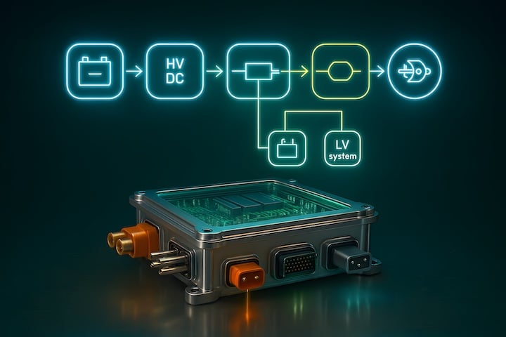
EV Power Electronics Control Unit. Image used courtesy of Adobe Stock (licensed).
The specific objectives of this technology are to minimize on-state resistance (RDS(on)), thereby reducing energy loss as heat during conduction, and to boost energy efficiency. This enables the development of more compact, low-consumption power supplies, EV chargers, and solar inverters. Furthermore, it aims to enhance switching speeds; thanks to its reduced gate charge, it can toggle rapidly, a critical factor for modern high-frequency electronics.
Maximizing Efficiency and Performance
HV SJ MOSFET technology represents a structural innovation that optimizes the relationship between breakdown voltage and on-resistance (RDS(on)).
While high-voltage power devices traditionally require a thick drift layer to withstand voltage—which can lead to higher resistance—SJ technology utilizes a charge balancing mechanism to bypass this constraint. By implementing alternating, highly doped vertical P and N columns in parallel, the charges effectively cancel each other out. This allows the device to maintain a high breakdown voltage while significantly reducing internal resistance through a more heavily doped conduction path.
By enabling higher doping levels in the N-region where current flows, RDS(on) is optimized for high-performance applications. This translates into minimal heat generation during conduction, substantially improving the overall energy efficiency of the system.
Due to its architectural efficiency, SJ technology achieves low resistance within a compact chip size. This design leads to lower parasitic capacitances and a decreased gate charge (Qg), allowing the transistor to toggle between 'on' and 'off' states with high precision and speed. Consequently, switching losses are minimized, which is essential for the performance of modern high-frequency power electronics.
In summary, by utilizing charge balancing to push the practical limits of silicon, HV SJ MOSFET technology simultaneously reduces conduction losses and enhances switching speeds. This combination allows for higher power density and superior thermal management, making it an indispensable solution for today’s most demanding high-efficiency energy systems.
High-Power Applications
HV SJ MOSFET technology is a key driver in the development of high-power applications, enabling the creation of more robust and efficient complex electronic systems. Let’s examine several of them.
Server and Telecom Power Supplies
Modern data centers demand extreme efficiency to reduce operational costs and cooling requirements. HV SJ MOSFETs enable power supplies to minimize conduction losses in the primary-side switching stages. Their high power density allows for more compact Switch-Mode Power Supplies (SMPS), maximizing the computing power available per rack unit.
Electric Vehicle (EV) Charging Stations
In the race for ultra-fast charging, efficiency is paramount to prevent overheating. Super Junction technology is utilized in the DC-DC conversion stages of charging piles. By reducing the total gate charge (Qg), these MOSFETs allow for higher switching frequencies, which in turn reduces the size of passive components like inductors and capacitors, leading to smaller and more reliable charging hardware.
Renewable Energy Inverters
Solar and wind energy systems rely on the precise conversion of DC to AC power. HV SJ MOSFETs improve the performance of solar micro-inverters and string inverters by ensuring that a higher percentage of harvested energy reaches the grid. Their robust design handles the high-voltage transients typical of outdoor energy environments while maintaining peak conversion efficiency.
Industrial Motor Drives
Industrial automation requires devices that can handle high inductive loads with high reliability. The low RDS(on) of SJ MOSFETs significantly reduces the heat dissipated by motor drive inverters, often simplifying the thermal management systems (heatsinks). This is critical for the development of sophisticated, high-efficiency factory robotics and heavy-duty machinery.

Solar inverter connected to a rooftop solar panel system. Image used courtesy of Adobe Stock (licensed).
Technical Challenges in Design
Despite its advantages, implementing Super Junction technology presents significant technical hurdles.
The primary challenge lies in the complex manufacturing process required to create deep, narrow, and perfectly balanced vertical P-columns, typically achieved through multiple epitaxial growth steps or deep trench filling.
Any charge imbalance between the N and P regions can lead to a drastic reduction in the breakdown voltage, making tight process control essential.
Additionally, managing high dv/dt and di/dt switching rates is critical, as the fast transition speeds can trigger unwanted electromagnetic interference (EMI) and voltage oscillations.
To mitigate the risks of EMI and oscillations, engineers employ several advanced design strategies. Active gate drivers are often used to precisely regulate switching speeds, while optimized external gate resistors (Rg) help dampen parasitic ringing.
Combined with rigorous PCB layout optimization to minimize parasitic inductance and the strategic use of RC snubber circuits, these techniques ensure stable operation even at the ultra-fast transition rates typical of HV SJ MOSFET technology.
Things to Keep in Mind
In conclusion, High-Voltage Super Junction MOSFET technology represents a definitive leap forward in power electronics, effectively overcoming the efficiency barriers of traditional planar structures. By leveraging the charge balancing mechanism, this technology achieves an optimal synergy between low on-resistance and ultra-fast switching speeds.
While it introduces specific design and manufacturing challenges, such as EMI management and complex fabrication, the implementation of advanced gate drives and optimized layouts successfully mitigates these hurdles. Ultimately, HV SJ MOSFETs remain an indispensable cornerstone for the development of the next generation of high-density, energy-efficient systems, from EV infrastructure to renewable energy and beyond.
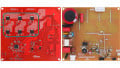
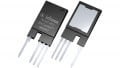
αMOS E2 600 V Super Junction MOSFET Platform
This platform features a high-voltage MOSFET product that meets the demands for high efficiency, power density, and robust performance across a wide range of applications, including servers, workstations, telecom rectifiers, solar inverters, motor drives, and industrial power systems.
To optimize mid- to high-power switched-mode power supplies (SMPS) and solar inverter designs, engineers must simultaneously address four critical constraints: efficiency, power density, system cost, and operational robustness. To achieve these benchmarks, HV SJ MOSFETs are now the primary choice for high-performance topologies.

The αMOS E2 high‑voltage super junction MOSFET platform. Image used courtesy of Alpha and Omega Semiconductor.
Announced in January this year, Alpha and Omega Semiconductor (AOS) designed the αMOS E2 HV SJ MOSFET platform with an enhanced intrinsic body diode to ensure reliability during hard commutation. This robust design protects the device against reverse recovery failures triggered by abnormal operating conditions, including short-circuits and start-up transients.
This platform and the first high-voltage MOSFET were designed to address the needs of traditional AC-DC power supplies, as well as DC-DC converters and DC-AC inverters, where achieving high power density and efficiency remains a critical challenge.
Leveraging AOS’ extensive MOSFET engineering expertise, the breakthrough capabilities of αMOS E2 HV SJ MOSFET platform solves these challenges enabling mid- to high-power application designers to effectively satisfy today’s and future power efficiency, durability and lower cost demands.