Facebook
 Google
 GitHub
 Linkedin
Reliability Challenges of Automotive-grade Silicon Carbide Power MOSFETs
In this article, a discussion is given about testing and related results of Silicon-carbide power MOSFETs for automotive applications. It reports mainly about trends, testing for wear of components, and testing for abnormal conditions. In summary, the main challenges are related to the cost of raw material, stable high-temperature operation, and high current density. However, the scenario is very dynamic and major changes are expected in the coming 2-3 years.
Because of the roadmaps worldwide toward society decarbonization, Power Electronics has boomed in the last twenty years. The reason for this is that the production, storage, and consumption of green energy are typically delocalized and need many more intermediate conversions than the ones from traditional fossil fuels. An example of an application of power electronics is electricity generation from wind. In such an application, reliability/security of supply is an intrinsic issue, along with challenges related to the efficiency, the cost of energy, the volume of converters, and their protection. Such systems are also typically more complex than the fuel-powered generators, hence they require special control efforts involving e.g. active- and reactive power management, resiliency against grid sags, and condition monitoring. Wind power is an example of an intrinsically power-electronics-enabled resource: the rotor speed of a wind turbine varies depending on the wind intensity, and transferring the gathered power to the grid at constant voltage and frequency would not be possible without power electronics. Another example comes from heavy-traction applications. ABB has presented a power-electronics traction transformer (PETT) in 2014 [1], where the goal was to replace the bulky and massive line-frequency iron transformer abord trains with a lighter and more efficient version based on power electronics. Mitsubishi has presented in the same year a retrofitting project for the Odakyu 1000 series train with the main power train based on SiC MOSFET modules [2].
In automotive, high-power modules are more and more demanded because of the increasing number of energy conversions need to run a modern hybrid or full-electric vehicle. Typically, three main converters are needed, namely the battery charger, the motor drive, and the auxiliary services converter. A higher frequency is a key challenge here, driven by demand for lower volume and higher efficiency. Other very important challenges are higher operating temperature and higher robustness, i.e. longer lifetime, short-circuit- and over-current withstanding capability, which often demand highly customized and integrated solutions.
Silicon carbide (SiC) is historically known for its mechanical properties, in particular its hardness, which is the second-highest in nature after diamond. As a semiconductor, SiC exhibits outstanding properties that overtake traditional silicon in terms of bandgap, breakdown electric field, saturation velocity, and thermal conductivity, which make out of it a great candidate to compete with silicon in the power electronics arena [3]. According to Yole/Systemplus, the SiC device market will have a compound annual growth rate of 40 % in the next 4 years [4]. Many players are present in the field, namely CREE/Wolfspeed, ROHM, ST, and Infineon, and almost all the power electronic component manufacturers have SiC devices in their portfolios. Nowadays, both discrete and module versions are available, and a 3rd generation is already available since 2017, which uses trench-gate technology. The landscape evolves very fast. For example, CREE has invested 1 billion USD in 2019 for a new production fab [5].

Figure 1: A typical power MOSFET chip structure. The drain contact is on the back side (not visible in the picture).
According to a recent market forecast from Yole Développement, the automotive market is to drive both the technological and market development in power electronics in the coming decade [6]. The expected operating life of automotive-grade components is around 15 years or 300,000 km, which can be translated into an expected life of 10,000 operation hours. In such a demanding scenario, it becomes crucial to test for reliability.
Power-cycle Testing of SiC MOSFETs
There are two fundamental approaches for packaging of power-electronic components, i.e. discrete packaging and module packaging. The first one has no electrical isolation, hence an external isolation layer must be provided, whereas the second one has a so-called direct-bond copper (DBC), or substrate, which provides this feature. Another main difference is the isolation filler, i.e. transfer-molding resin in discrete packaging, and silicone gel in modules, although there may be found some different solutions, especially in custom designs. However, in either case, one or more semiconductor devices (“chips”) are present, which are the core of the power electronic device. A chip has typically a sandwich-like structure, where a top layer made of metal is the source contact, and the bottom layer is the drain contact (see Figure 1). The bottom layer is glued on the substrate with a solder paste or, more recently, with a silver-sintered layer. The top layer is usually contacted using metal bond wires.
![Figure 2: Wafer price per area of several semiconductor materials for power electronics [7].](https://eepower.com/uploads/articles/Reliability_Challenges_of_Automotive-grade_Silicon_Carbide_Power_MOSFETs_Fig2_Fixed.JPG)
Figure 2: Wafer price per area of several semiconductor materials for power electronics [7].
Figure 2 shows the cost per square inch of modern semiconductor materials [7]. As it can be noted, the SiC price is still above 10x higher than silicon, which constrains the development of devices with this technology. Such a constraint forces component designers to reduce significantly the chip area, which, in turn, produces two other consequences: a) a smaller area for bond-wire footprints, and b) a higher power density, hence a higher temperature swing. The two above issues are related to packaging. On top of them, an issue intrinsically related to the SiC semiconductor itself needs to be mentioned, i.e. the larger bandgap requires a higher electric field at the gate oxide that can cause electrical instabilities.
Degradation in SiC MOSFETs can occur at two main levels, namely packaging- and semiconductor level.
Packaging Degradation
The increase in the semiconductor current density implies an increase in the bond-wire current density. To investigate such an effect, Figure 3 displays the usage of a Kelvin-source connection for monitoring the bond-wire voltage drop during power cycling [8]. Two SiC-MOSFET modules, namely A and B, were subjected to power-cycling tests under the conditions reported in Table 1. The maximum and minimum temperature, the temperature swing, and the timing were kept the same. The only difference was the load current. The results show that the current density has an impact on the series resistance (see Table 2). The sample with the higher current has shown a larger increase in the series resistance, although all the other testing parameters were kept the same.
![Figure 3: Photograph (left) and schematic (right) of Kelvin-source connection for testing the bond-wire voltage drop during power cycling [8].](https://eepower.com/uploads/articles/Reliability_Challenges_of_Automotive-grade_Silicon_Carbide_Power_MOSFETs_Fig3.JPG)
Figure 3: Photograph (left) and schematic (right) of Kelvin-source connection for testing the bond-wire voltage drop during power cycling [8].
| Test Parameters | Module A | Module B |
| Tj, max | 125 °C | 125 °C |
| Tj, min | 65 °C | 65 °C |
| ΔTj | 60 °C | 60 °C |
| tON/tOFF | 2s / 4s | 2s / 4s |
| Load current | 24 | 12 |
Table 1. Conditions used for assessing the effects of current density on bond-wire liftoff failure [8]
| 12A | 24A | |||
| mΩ | 0 cycles | 70k cycles | 0 cycles | 70k cycles |
| Average | 3.07 | 4.03 | 2.70 | 4.68 |
| Std deviation | 0.51 | 1.13 | 0.34 | 0.87 |
Table 2. Series resistance of bond wires at end of life (around 70,000 cycles) in the case ILOAD = 12 A and ILOAD = 24 A [8]
Semiconductor Degradation
Degradation at the semiconductor level happens mostly in connection with high-temperature operations. Because of the wider bandgap compared to silicon, silicon carbide would exhibit a larger threshold voltage than silicon with the same gate oxide thickness. This is not acceptable from an application point of view, as gate drivers and circuitry are nowadays widely standardized in the range 10 V to 20 V. This market constraint calls for a thinner gate oxide of SiC MOSFETs compared to silicon, which in turn makes oxide quality more critical. At high temperatures, the probability of having energetic (“hot”) electrons through the oxide becomes more and more significant due to the well-known Fowler-Nordheim tunneling effect [9]. Figure 4 displays this condition, where a hot electron through the channel has energy enough to pass through the oxide and it either gets to the gate terminal or gets trapped into the gate layer. In this latter case, a permanent negative gate charge adds up to the device, which increases its threshold voltage. This phenomenon is regenerative, as the higher the threshold voltage, the higher the losses, and the higher the losses, the higher the temperature. Figure 5 displays the degradation curves obtained for both the semiconductor chip and its bond-wires during a power-cycling experiment with a maximum temperature of 175 °C. Although a bond-wire degradation is observed, the semiconductor chip fails independently of it. The degradation observed is a typical thermal-runaway phenomenon [9].
![Figure 4: Effects of hot-electron trapping related to the Fowler-Nordheim tunneling mechanism [9].](https://eepower.com/uploads/articles/Reliability_Challenges_of_Automotive-grade_Silicon_Carbide_Power_MOSFETs_Fig4.JPG)
Figure 4: Effects of hot-electron trapping related to the Fowler-Nordheim tunneling mechanism [9].
Testing for Abnormal Conditions
Highly-reliable applications, such as energy production from renewables require an expected life of 20 or more years. In this time horizon, random failures cannot be neglected. Random failures are related to abnormal events occurring during the component’s life, such as grid voltage ride-through, overloads, short-circuits, and lightnings.

Figure 5: Degradation curves during power-cycling of a commercial SiC MOSFET module, with a maximum temperature of 175 °C. Top: voltage drop across the semiconductor chip. Bottom: voltage drop across bond-wires [9].
Short-circuit is one of the greatest challenges. Testing against shortcircuit events is risky, as such events often end up in a catastrophic failure. To prevent this and to allow post-failure analysis, a protection circuit must be used. Figure 6 shows a principle schematic of a non-destructive tester for short-circuit conditions [10]. A power supply VDC charges preliminary a capacitor bank CDC up to the test voltage. The series protection is made up of parallel-connected IGBT power switches, which are operated simultaneously. The series protection is fired earlier than the device under test (DUT) and is turned off right after it. In this way, in the case of failure and loss of control, the energy dissipated on the DUT is largely limited. The timing should be finely tuned in the fraction-of-microsecond scale, therefore an FPGA hardware generates the test signals. All the waveforms are sampled using an oscilloscope and collected with a personal computer.

Figure 6: Principle schematic of a setup for short-circuit testing of power semiconductors.
![Figure 7: Short-circuit waveforms for a commercial 1.2 kV, 300 A SiC MOSFET module. Yellow: drain voltage [200 V/div]; Blue: drain current [1 kA/div]; Pink: gate voltage [5 V/div]. Time: [1 us/div]. [11]](https://eepower.com/uploads/articles/Reliability_Challenges_of_Automotive-grade_Silicon_Carbide_Power_MOSFETs_Fig7.JPG)
Figure 7: Short-circuit waveforms for a commercial 1.2 kV, 300 A SiC MOSFET module. Yellow: drain voltage [200 V/div]; Blue: drain current [1 kA/div]; Pink: gate voltage [5 V/div]. Time: [1 us/div]. [11]
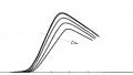
Figure 7 displays the rupture waveforms of a commercial SiC MOSFET after a 3-microsecond short-circuit event [11]. The turn-off sequence appeared to be safe in the experiment. However, after about 2 microseconds after the turn-off, a sudden increase in the drain current occurred, evidencing that an instability took place and led the device to destruction. A post-failure analysis on the same unit demonstrated a burnt spot on one chip (see Figure 8). Another example is given by the waveforms showed in Figure 9. In this second case, a failure occurred during turn off. A possible interpretation of such phenomena is related to the dependence of the on-state characteristics on the temperature. Figure 10 shows a superimposition at two different temperatures of the characteristics taken from the datasheet of the commercial device used for the tests. At low gate voltages, e.g. VGS = 10 V, SiC MOSFETs exhibit a negative-thermal-coefficient behavior, which means that the current increases when the temperature increases. Although such a so-low voltage level is unusual in normal operations, it may appear in the case that a significant current is triggered through the gate oxide because of a high temperature, ending up in an electro-thermal instability.
To prove the above hypothesis, a post-failure analysis has been done at much lower short-circuit energies, so that the device under test was not severely damaged. The observation done showed clear evidence of a crack occurring through the field oxide and possibly leading to a conductive path between the gate terminal and the source metallization [12].
Status and Prospects
Cost is certainly the major hurdle for a broad diffusion of SiC MOSFETs in power-electronics applications. A lower cost would mean gaining one more design degree of freedom. The chip area could be not a constraint anymore and could allow the full exploitation of the SiC material potential, especially from a reliability standpoint.
With no doubt, the temperature is the second hurdle. Despite high expectations, operations are still limited to Tj, max = 150 °C in the greatest number of cases. To conquer the automotive market (worth 1.5 B$, CAGR 3,4% in 2017 [13]), a 200 °C stable operation is demanded.
The third hurdle is new interconnection concepts. Temperature swing has become a constraint at the solder layer, too. New and cheap concepts are demanded to enable the transition toward SiC technology.
However, the scenario is very dynamic. As mentioned above, the first world SiC wafer manufacturer Cree invested 1B$ in a new wafer fab in May 2019 [5]. Danfoss has now an enlarged portfolio with Danfoss Bond Buffer® technology (copper wire bonding) [14]. Major changes have still to be expected in the coming 2-3 years.

Figure 8: Post-failure analysis on a commercial SiC MOSFET module after a short circuit test, showing a burnt spot on a chip.
Conclusion
I have discussed the main reliability challenges of state-of-the-art SiC MOSFETs aimed at automotive applications. As take-home messages, I would highlight:
1) the automotive applications are expected to drive the power electronics scenario in the coming decade. This means that whatever the new technology, it has to comply with the current- and the coming automotive standards, in particular related to high-temperature operations.
2) Wear testing in Silicon Carbide components evidences two distinct failure mechanisms, i.e. bond-wire lift-off and threshold voltage shift. Current density plays a major role in bond-wire lift-off, whereas temperature mostly affects the threshold voltage shift. A technology effort is demanded at both levels.
3) Abnormal operations are as important as normal ones for SiC reliability assessment and are currently the most limiting performance.
![Figure 9: Short-circuit waveforms for a commercial 1.2 kV, 300 A SiC MOSFET module. Green: drain voltage [200 V/div]; Pink: drain current [1 kA/div]; Blue: gate voltage [10 V/div]. Time: [1 us/div].](https://eepower.com/uploads/articles/Reliability_Challenges_of_Automotive-grade_Silicon_Carbide_Power_MOSFETs_Fig9.JPG)
Figure 9: Short-circuit waveforms for a commercial 1.2 kV, 300 A SiC MOSFET module. Green: drain voltage [200 V/div]; Pink: drain current [1 kA/div]; Blue: gate voltage [10 V/div]. Time: [1 us/div].
![Figure 10: Dependence of on-state characteristics of a SiC commercial device on the temperature. Black: 25 °C; Red: 150 °C [11].](https://eepower.com/uploads/articles/Reliability_Challenges_of_Automotive-grade_Silicon_Carbide_Power_MOSFETs_Fig10.JPG)
Figure 10: Dependence of on-state characteristics of a SiC commercial device on the temperature. Black: 25 °C; Red: 150 °C [11].
![Figure 11: Post-failure analysis on a commercial discrete SiC MOSFET after a repetitive short-circuit test, showing a crack in the field oxide [12].](https://eepower.com/uploads/articles/Reliability_Challenges_of_Automotive-grade_Silicon_Carbide_Power_MOSFETs_Fig11.JPG)
Figure 11: Post-failure analysis on a commercial discrete SiC MOSFET after a repetitive short-circuit test, showing a crack in the field oxide [12].
This article originally appeared in Bodo’s Power Systems magazine.
References
[1] ABB, “A power-electronic traction transformer (PETT).”
[2] Compoundsemiconductor.net, “Mitsubishi Electric To Supply SiC Power Inverter To Odakyu Railway.”
[3] G. Majumdar, Tatsuo, and Oomori, “Some Key Researches on SiC Device Technologies and their Predicted Advantages,” 2009.
[4] Yole Developpement, “Power SiC 2019: Materials, Devices, and Applications by Yole Développement.” www.yole.fr (accessed Nov. 04, 2020).
[5] CREE, “Cree to Invest $1 Billion to Expand Silicon Carbide Capacity,” [Online]. Available: https://www.cree.com/news-events/ news/article/cree-to-invest-1-billion-to-expand-silicon-carbidecapacity.
[6] Yole Developpement, “Status of the Power Electronics Industry - Overview.” http://www.yole.fr (accessed Nov. 04, 2020).
[7] i-Micronews, “6’’ and Below: Small-Dimension Wafer Market Trends 2020 - i-Micronews.” https://www.i-micronews.com (accessed Nov. 04, 2020).
[8] H. Luo, F. Iannuzzo, N. Baker, F. Blaabjerg, W. Li, and X. He, “Study of Current Density Influence on Bond Wire Degradation Rate in SiC MOSFET Modules,” IEEE J. Emerg. Sel. Top. Power Electron., vol. 8, no. 2, pp. 1622–1632, Jun. 2020, doi: 10.1109/ JESTPE.2019.2920715.
[9] H. Luo, F. Iannuzzo, and M. Turnaturi, “Role of Threshold Voltage Shift in Highly Accelerated Power Cycling Tests for SiC MOSFET Modules,” IEEE J. Emerg. Sel. Top. Power Electron., vol. 8, no. 2, pp. 1657–1667, Jun. 2020, doi: 10.1109/JESTPE.2019.2894717.
[10] L. Smirnova, J. Pyrhonen, F. Iannuzzo, R. Wu, and F. Blaabjerg, “Round busbar concept for 30 nH, 1.7 kV, 10 kA IGBT non-destructive short-circuit tester,” 2014, doi: 10.1109/ EPE.2014.6910712.
[11] Wolfspeed, “CAS300M12BM2 datasheet.” www.wolfspeed.com.
[12] H. Du, P. D. Reigosa, F. Iannuzzo, and L. Ceccarelli, “Investigation on the degradation indicators of short-circuit tests in 1.2 kV SiC MOSFET power modules,” Microelectron. Reliab., vol. 88– 90, pp. 661–665, Sep. 2018, doi: 10.1016/j.microrel.2018.06.039.
[13] Yole Developpement, “Power MOSFET 2017: Market and Technology Trends - 2017.” [Online]. Available: www.yole.fr. [14] Danfoss, “Danfoss Bond Buffer (DBB).” [Online]. Available: http:// files.danfoss.com/download/Drives/DKSPPB402A202_Danfoss_ Bond_Buffer.pdf.
About the Author
Francesco Iannuzzo received his M.Sc. degree in Electronic Engineering and a Ph.D. degree in Electronic and Information Engineering at the University of Naples Federico II, Italy. He worked as a Professor at the University of Naples Federico II.
Related Content