Facebook
 Google
 GitHub
 Linkedin
The eGaN FET Supply Chain
This article discusses the supply chain of silicon MOSFETs and eGaN FET and offers their capital investment and product costs and effect against MOSFETs.
Key Take Aways
- GaN technology is compatible with low-cost silicon integrated circuit infrastructure already in place, allowing GaN technology to leverage billions of dollars of underutilized semiconductor supply chain.
- eGaN FETs eliminate one standard element in the semiconductor supply chain – the external plastic package. On average, the plastic package accounts for approximately 50% of the overall cost of a silicon MOSFET.
- Since the majority of the supply chain is in place and is underutilized, eGaN FET production can expand rapidly with very limited investment in new capital.
- Partly due to leveraging the underutilized existing semiconductor supply chain, over the next three years we expect the production costs of GaN transistors to go below the costs of silicon power MOSFETs.
In the past issues of Technology Driving Markets, we have presented a path from the basic properties of a gallium nitride crystal, to how this material, when transformed into an eGaN® FET, can enable some amazing new end-use applications, such as wireless power transfer, LiDAR, and envelope tracking. Extending beyond the power transistor market, eGaN FETs have the potential to infiltrate the higher value markets for power integrated circuits and analog IC’s. These markets, added to the power transistor market, total over $40B annually.
We now turn our attention to the supply chain needed to support the growth of eGaN technology. Hundreds of billions of dollars have been spent to make the silicon technology supply chain incredibly efficient. How can GaN transistors compete against this huge installed base of silicon-based production?
The Silicon MOSFET Supply Chain
Today’s power MOSFET follows a supply chain model as shown in figure 1. The starting point is the growth of a silicon crystal, followed by the growth of a thin layer of epitaxial silicon. These wafers are then processed through many tens, or even hundreds, of steps to produce a completed wafer with hundreds (or thousands) of individual transistors. Figure 2 is an image from the interior of a wafer fabrication facility showing the clean room and equipment common to semiconductor manufacturing. New wafer fabrication and test facilities like this cost several billions of dollars each to build and equip.
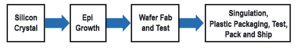
Figure 1: The typical power MOSFET supply chain. Each block is performed in a different facility, often on different continents.
Testing is the next step where bad devices are identified to be removed at a later step. Following testing, the finished wafers are sent to a different facility to be saw-cut (singulated) into individual devices. Once singulated, the good devices are assembled into plastic packages, tested again to identify further rejects, packed and shipped
to customers. Figure 3 is an image from the interior of an assembly facility showing the cleanroom and assembly equipment. On average, assembling MOSFETs into plastic packages account for about 50% of the total product cost.
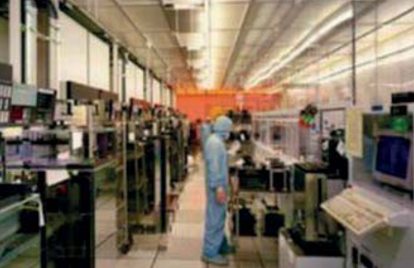
Figure 2: Image from the interior of a wafer fabrication clean room.

Figure 3: Image from the interior of a packaging clean room. About 50% of the cost to manufacture a power MOSFET is in the packaging step.
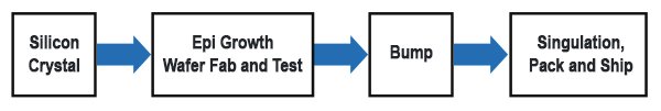
Figure 4: The current eGaN FET supply chain. Each block is performed in a different facility. The last three steps are all in the same city in Taiwan.
The eGaN FET Supply Chain
The current eGaN FET supply chain is shown in figure 4. Like the power MOSFET, the starting point is the growth of a silicon crystal. Instead of an epitaxial silicon layer, an epitaxial structure of aluminum nitride, aluminum gallium nitride, and gallium nitride is grown (This is called a heteroepitaxial structure). This growth is the only step that requires equipment specialized for GaN transistors. Both the epitaxial growth and the wafer fabrication today take place inside a commercial silicon foundry originally built in the late 1980s to manufacture DRAMs. This kind of trailing-edge capacity is widely available in the industry, and is perfectly adequate for producing state-of-the-art eGaN FETs because this technology is not as driven by smaller geometries. eGaN FETs also require far fewer process steps in the wafer fabrication process compared with advanced power MOSFETs.
As with MOSFETs, a testing step, whereby faulty die are identified for future segregation, follows wafer fabrication. Unlike the MOSFET, eGaN FETs, while still in wafer form, have a protective plastic coating applied and solderable bumps screen printed to form the electrical contacts to the outside world. This relatively low-cost sequence of steps for producing an eGaN FET replaces the costly and bulky plastic package needed for the silicon MOSFET.
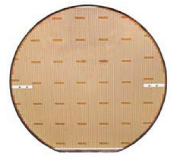
Figure 5: Completed eGaN FET wafer. There are about 10,000 transistors on this wafer. The next step is singulation, where the wafer is saw-cut and the individual transistors that passed testing are separated from failed devices.
At this point, the eGaN FET wafer looks like the one shown in figure 5. There are about 10,000 transistors on this wafer. A comparable silicon MOSFET wafer would have only 2,000 to 3,000 devices. Singulation, packing and shipping are the final steps.
In the next couple of years, the bump, singulation, test, pack and ship steps will be integrated into the wafer fabrication facility as illustrated in figure 6. This consolidation will save cost and reduce the cycle time in the supply chain. It also improves flexibility and responsiveness to market fluctuations and reduces the amount of working capital needed to expand.
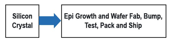
Figure 6: The future eGaN FET supply chain. All steps following silicon crystal growth are expected to be performed in the same facility.
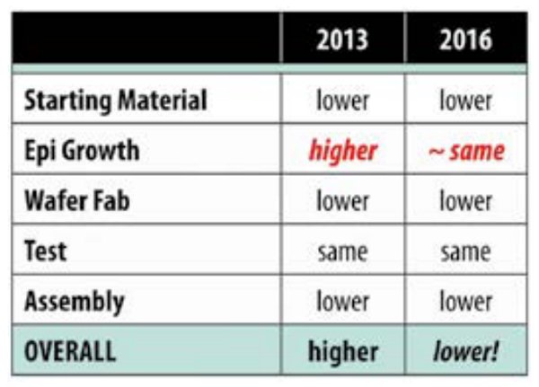
Figure 7: Cost comparison between eGaN FETs and power MOS- FETs. In 2016, we expect eGaN FETs to cost less to produce than a power MOSFET with similar ratings.
Capital Investment and Product Cost
With the exception of the machines needed to grow the epitaxial GaN layers on top of silicon, all of the machinery needed to manufacture eGaN FETs is standard, trailing-edge equipment used to manufacture billions of silicon integrated circuits today. History shows that trailing- edge silicon wafer capacity is chronically abundant. The use of highly available and very mature capacity greatly reduces the amount of capital and the risk required to produce eGaN FETs in high volume.
How does this all add up? The cost comparison between a power MOSFET and an eGaN FET with similar voltage and on-resistance specifications (as discussed in the May 2014 Technology Driving Markets article) is illustrated in figure 7. With the introduction of next-generation epi growth equipment, as well as the benefits of scale, eGaN FETs should be less costly to produce than the venerable power MOSFET. Couple this reduced production cost with the relatively low cost and risk needed to rapidly expand the supply chain, and the thesis that the eGaN FET will dethrone the power MOSFET as the dominant power conversion transistor becomes quite persuasive.
About the Author
Alex Lidow PhD joined International Rectifier as an R&D engineer and is the co-inventor of the HEXFET power MOSFET, a power transistor that displaced the bipolar transistor and launched modern power conversion. Over the 30 years Dr. Lidow was at IRF, his responsibilities grew from engineer to head of R&D, head of manufacturing, head of sales and marketing, and finally CEO for 12 years. In addition to holding many power MOSFET and GaN FET patents, Alex has authored numerous publications; most recently he co-authored the first textbook on GaN transistors, GaN Transistors for Efficient Power Conversion. In 2004 he was elected to the Engineering Hall of Fame, and in 2005 IRF, under his leadership, International Rectifier was named one of the best managed companies in America by Forbes magazine. Dr. Lidow earned a Bachelor of Science in Applied Physics from the California Institute of Technology and a doctorate in Applied Physics from Stanford University.
This article originally appeared in the Bodo’s Power Systems magazine.