Facebook
 Google
 GitHub
 Linkedin
Solving the Power Density Challenge
This article gives insight on Source-Down packaging technology, a key enabler for delivering the required power density to feed the power-hungry megatrends like artificial intelligence.
Artificial intelligence (AI), smart cities, and autonomous driving are only a couple of megatrends that impact mankind and transform our way of living. They also pose some tough challenges to current state-of-the-art technologies in many related disciplines.
The Challenge
One of the biggest bottlenecks in enabling AI and keeping up with the calculation and storage needs in the cloud is power management. More specifically, the power density of the power converters used to fuel the processors and ASICs in the system.
The “Open Compute Project” (OCP) attempts to address these challenges by defining new standards in the power architecture, moving from the traditional 12 V intermediate bus voltage up to 48 V. This significantly reduces transmission losses and enables a more efficient way to transfer power to the payload (i.e., AI ASIC / GPU / CPU or SOC). The power levels of AI accelerator modules are already exceeding 750 W with currents as high as 1000 A (@ 0.75 V core voltage). When looking at as many as eight of those modules on one mainboard, the power ratings and thermal management efforts become mind-boggling.
Current State-of-the-Art
With the introduction of the 48 V power-delivery architecture, efficiency improvements in the power conversion process are becoming vital. A two-stage conversion is commonly adopted to satisfy the requirements for high voltage ratios with challenging transient requirements. LLC resonant converters are widely used as intermediate bus converters (IBCs) because of zero-voltage switching (ZVS) at the primary 48 V side and zero-current switching (ZCS) on the secondary 12 V side. If isolation is not required, a conversion based on switched-capacitor converters (ZSCs) can be adapted to further improve performance and increase power density.

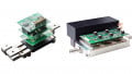
Figure 1: A general OAM board from Infineon
For the new open compute accelerator module (OAM), depicted in Figure 1, power density is a key parameter and the main challenge for the new 48 V power-delivery architecture. The available footprint area for the IBC and multiphase buck system is visualized in Figure 2.

Figure 2: The OAM dimensions and footprint requirements for a 48 V power-delivery system
To meet the footprint requirements, high switching frequency operation is needed both in the first and second stages. However, high-frequency operation, especially on the VRM stage (i.e., 1.5 … 2 MHz), leads to higher losses (i.e., switching, gate-driving, and conduction losses).
Reducing the input voltage on the VRM stage down to 6 V enables a reduction of the footprint size while maintaining high efficiency. For higher conversion ratios, an IBC based on a switched capacitor topology becomes too complex and bulky in terms of floating driver requirements and the number of switches and ceramic capacitors.
To implement a high step-down ratio IBC, a transformer-based topology such as a full-bridge LLC resonant converter is widely used regardless of galvanic isolation requirement. While there are many advantages to using a transformer-based topology, there are also some drawbacks.
For example, the step-down ratio is determined by the turn winding ratio between the primary side and secondary side and in an LLC center-tapped resonant converter the utilization of the copper is not optimized. To overcome the limitations of I²R losses in the transformer, Infineon has introduced a hybrid switched-capacitor (HSC) converter that combines the benefits of switched capacitor converters and the high step down ratio capability of a magnetic device. By transferring the energy through capacitors and a magnetic device, the efficiency and power density can be improved significantly. This enables the required power density for the OAM.
HSC Converter
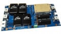
In resonant converters like the LLC, the switching frequency needs to be close to the LC resonance for soft switching. Moreover, the entire energy is transferred through the transformer, increasing the overall losses. A converter topology whose efficiency varies heavily with the component mismatch is not viable for mass production without extra compensation efforts. To overcome these issues a novel approach based on the HSC topology dual-phase resonant converter is proposed by Infineon. As illustrated in Figure 3 the HSC is formed by 6 MOSFETs divided into two legs, connected through two flying capacitors and a magnetic device called a multi-tapped autotransformer (MTA). The MTA is formed out of 4 windings connected in series sharing the same magnetic core. High-frequency operation is enabled by ZVS operation with the magnetizing inductance of the MTA.

Figure 3: HSC converter topology
The HSC provides an unregulated voltage rail which depends on the turn ratio between N1 and N2. The topology is driven by two symmetrical PWMs: H (i.e., Q1, Q3, and Q5 are ON with Q2, Q4, and Q6 OFF) and L (i.e., Q1, Q3, and Q5 are OFF with Q2, Q4, and Q6 ON). An introduced dead-time between the states enables load-independent ZVS operation. The HSC can run above- and below-resonant frequency without influencing the ZVS operation. Therefore, the overall system performance can be kept at a high level regardless of component tolerances.
One of the key enablers for high efficiency and high power density of the HSC is the use of low-voltage rated MOSFETs with better figure of-merits (FOMs). For example, in an 8:1 configuration running from a 48 V rail, 25 V-rated MOSFETs for Q3 and Q6 can be used.
The Source-Down Concept: Pushing the Envelope in Power Density
Addressing the power density challenges requires innovation at the component level with advancements in resonant topologies. With the introduction of Infineon´s Source-Down package technology, the IQE006NE2LM5 further enhances electrical and thermal performance, enabling the power density needed in modern datacenter applications. The main benefits of the innovative package include:
-
30 percent lower RDS(on), decreasing I²R losses
-
Lower package-related parasitics, reducing the FOM and leading to lower switching losses
-
Lower Rthjc, optimizing the distribution of the generated heat from the package
-
The thermal pad is located on the source pin, thus enables optimized layouts where the large GND area can be utilized as a heatsink

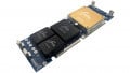
Figure 4: The thermal behavior of the HSC at 450 W from 48 V input at Tamb = 24°C and v = 3.3 m/s: a) with BSZ011NE2LS5I, b) with IQE006NE2LM5
To compare the performance benefits, two versions of an 8:1 HSC was built, using today’s standard Drain-Down device (BSZ011NE2LS5I) on one board and the new Source-Down device (IQE006NE2LM5) on the other. Figure 4 compares the thermal performance of the devices. The traditional package shows a hot-spot (Figure 4 a) that is eliminated with the use of the new source-down package (Figure 4 b). The surface temperature of the MOSFET is significantly improved, showing a 9°C difference compared to the Drain-Down device. Figure 5 illustrates the efficiency comparison (including auxiliary losses). The higher efficiency of the system featuring the new source-down device leads to a significant increase in power density as well.

Figure 5: The HSC converter efficiency from 48 V to 6 V, including auxiliary losses, with BSZ011NE2LS5I (in blue) and with IQE006NE2LM5 (in red) at Tamb = 24°C and v = 3.3 m/s
From all of the above-mentioned benefits and performance measures, one can easily conclude that this novel solution, the Source-Down packaging technology, is a key enabler for delivering the required power density to feed the power-hungry megatrends like artificial intelligence.
About the Authors
Bastian Lang holds a Dipl. -Ing in Electrical and Computer Engineering from the Regensburg University of Applied Sciences and is skilled in the field of power electronics, power management and product development. He is currently the manager of product marketing at Infineon Technologies. Lang's focus is on power management and product development. Lang worked with ROHM Semiconductor, the PULS Group, and Integrated Device Technology before joining the Infineon Technologies team.
Roberto Rizzolatti holds a Master's Degree in Electrical and Electronics Engineering earned at the University of Udine and is skilled with MatLab SimuLink and SIMetrix. He currently works as a System Innovation Engineer at Infineon Technologies since November 2018.
Christian Rainer is a DC/DC system innovation engineer with Infineon Technologies Austria AG. Rainer has two patents: Current Sensing in an Electromagnetic Component Using an Auxiliary Winding Stub Method and Apparatus for Zero-Current Switching Control in Switched-Capacitor Converters.
This article originally appeared in the Bodo’s Power Systems magazine.