Facebook
 Google
 GitHub
 Linkedin
“AllI n One” DIPIPM Series for Compact Inverter Designs
This article introduces Mitsubishi Electric's DIPIPM+TM series, a Converter-Inverter-Brake modules, to help reduce the cost and size of inverter design.
A novel family of compact Intelligent Converter-Inverter-Brake-modules was developed. This new DIPIPM+TM series incorporates optimized IGBT- and FWDi-chips, low voltage and high voltage driver ICs in a compact transfer molded dual-inline package. The new DIPIPM+TM series is providing smart answers on the 2 key questions a designer is facing when developing a new inverter design: How to reduce the system cost? How to reduce the inverter size by compact design?
Introduction
The newly developed DIPIPM+TM series was introduced recently [1]; [2]. It consists of 6 different module ratings in 2 selectable configurations: Converter-Inverter-Brake-topology (see Figure 1) or Converter-Inverter-topology (see Figure 2).
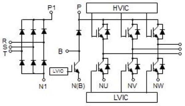
Figure1: DIPIPM+TM line-up and circuit diagram with brake

Figure 2: DIPIPM+TM line-up and circuit diagram without brake
All the DIPIPM+TM modules are encapsulated into the same very compact dual-inline package according to Figure 3.

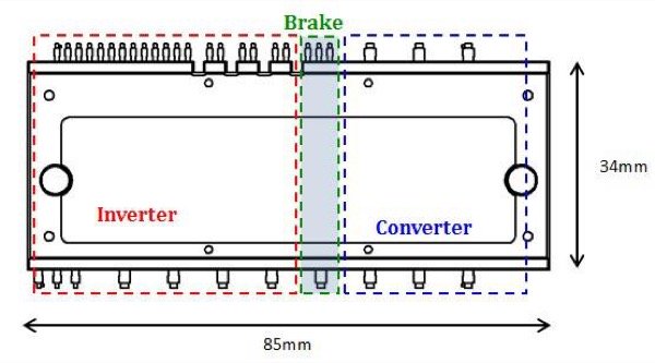
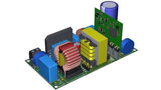
Figure 3 DIPIPM+TM photo & dimensions
An overview of the implemented DIPIPM+TM functions [2] is shown in the block diagram in Figure 4:
- The P-side IGBTs are driven by an HVIC with input signal conditioning, level shifter and under-voltage lock-out
- The P-side control power is provided from a single external 15V supply via integrated bootstrap diodes and resistors
- The N-side IGBTs are driven by LVIC with input signal conditioning, SC-protection and under-voltage lock-out
- The LVIC also contains an analogue temperature signal VOT and is generating a fault output Fo in case of protection trip
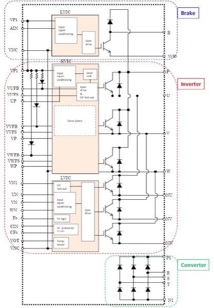
Figure 4: DIPIPM+TM internal block diagram
Cost reduction
When developing a new general-purpose inverter reducing the system cost is a key motivation. Basically, 3 cost factors must be considered: a) development cost; b) material cost and c) manufacturing cost. All 3 factors are addressed by the new DIPIPM+TM series.
Reducing Development Cost and Time
The DIPIPM+TM is an “all-in-one” inverter module, consisting of a 3-phase input rectifier, a brake chopper and a 3-phase output inverter having all dedicated gate driver and protection functions integrated (see Figure 4). For reducing the development cost (and respectively the time to market of the new inverter) a plug-and-play evaluation board has been developed [3], see Figure 5.
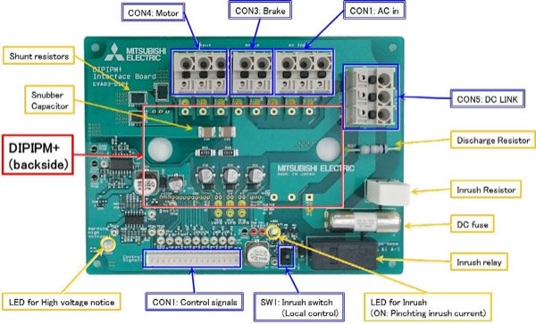
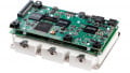
Figure 5: DIPIPM+TM evaluation board. The position of DIPIPM+TM backside the PCB is indicated with red color
It contains all required peripheral components to get quickly an inverter prototype running with the DIPIPM+TM: snubber capacitor; nonisolated interface connector to the microcontroller; shunt resistors and comparators for overcurrent protection; bootstrap capacitors for p-side IGBTs; inrush current limiter and numerous test points for acquiring the signals. An easy test setup with the DIPIPM+ TM Evaluation Board is shown in Figure 6.
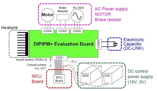
Figure 6: Test setup using the DIPIPM+TM evaluation board
All power connections to AC-line; brake resistor; motor and DClink capacitor can be done solder-less. The DIPIPM+TM is the only component mounted from the bottom side of the PCB. Thus, even with such first functional prototype arrangement, the best fitting heat sink structure can be verified experimentally in real inverter operation. Particularly such early heat sink confirmation may help reducing the total development time of a new inverter design.
Material Cost Reduction
Several aspects how to reduce material cost by using DIPIPM+TM will be discussed next.
A. By using HVIC with level shifting technology and bootstrap power supply only one external +15V control power supply is needed. As the microcontroller is operating DC-link N-potential no isolation is needed between high voltage part and low voltage control part of the inverter. In this way, the additional cost for individual +15V control power supplies and signal isolation for each IGBT-channel is eliminated. Only 3 bootstrap capacitors need to be added at the PCB for providing the control power to the p-side IGBTs. The safety isolation to the outside world should be implemented by the inverter designer into the HMI (human-machine interface), which can be done much more cost-efficiently, than individually for each IGBT-channel.
B. For vector control, the instantaneous values of inverter output currents must be monitored. By utilizing the open n-side emitters in DIPIPM+TM the inverter phase currents can be measured by shunts in each phase. The same shunt signals can be used to for tripping the DIPIPM+ TM short circuit protection (see Figure7). In this way, the higher cost for individual AC-current sensors in each inverter output can be avoided.

Figure 7: Using open emitter shunts for SC-protection and phase current sensing
C. New inverter designs must meet the EMC-requirements according to EN 61800-3. For this purpose, either external or inverter-built-in EMC-filters are used. Reducing the EMC-filter cost is an efficient way for reducing the total cost for an inverter system.
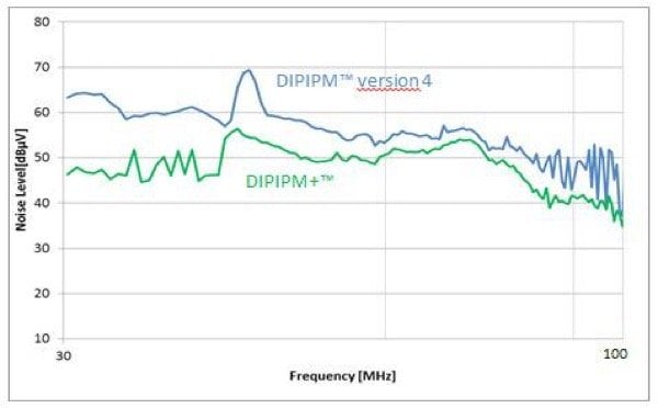
Figure 8: Radiated noise of DIPIPM+TM vs. previous generation DIPIPM TM Version 4
In Figure 8 the radiated EMI noise of DIPIPM+TM is compared with the previous IPM-generation (DIPIPM TM Version 4) under real inverter operation conditions. Due to the reduced noise emission of the new DIPIPM+TM a remarkable reduction of EMI-filter efforts can be achieved.
D. The package size of DIPIPM+TM is about 35% reduced compared with today’s state-of-the-art 1200V DIPIPM TM. The well-organized pinout of the DIPIPM+TM permits using a low-cost double layer PCB to ensure low inductive connection of the power stage to the DC-link capacitor. Furthermore, the Dual–Inline structure itself enables an easy signal and power terminals separation at the PCB (see Figure 9) thus allowing a very compact and thereby low-cost PCB-design.

Figure 9: Pin terminal assignment of DIPIPM+TM
E. The package of DIPIPM+TM is the same for all current ratings between 5A and 35A/1200V. This allows the use of the same PCB platform for different inverter ratings and topologies. Reducing the variety of inverter frame sizes is one way of reducing material cost.
F. The all-in-one DIPIPM+TM concept reduces the space needed for the 3-phase inverter part by about 50% compared with today’s state-of-the-art 1200V DIPIPM, see Figure 10. In combination with optimized low loss IGBT-and FWDi-chips, this leads to a remarkable reduction of heatsink size and thereby also to reduced dimensions of the inverter housing itself. As a result, the cost for mechanical parts in the inverter construction can be reduced.

Figure 10: Conventional Large DIPIPM Ver.6 versus DIPIPM+TM
Reducing the manufacturing cost
A. The high integration rate of DIPIPM+TM drastically reduced the parts count. Compared with an inverter design using a conventional 7in1 IGBT-module with separate driver ICs and a 3-phase input rectifier module the number of components to be placed at the PCB is reduced to about half, thus reducing the PCB-manufacturing cost.
B. Another cost reduction factor is the simple flow soldering process that can be used for the DIPIPM+TM assembly to the PCB. As the inverter bridge, the brake transistor and the input rectifier are integrated into the same module package no special care for height adjustment during soldering must be taken for controlling the distance between PCB and heat sink; simple spacers will be sufficient. If for example 2 separate power modules for inverter and input rectifier are used at the same PCB, in this case, individual height adjustments for each module are necessary during soldering process for ensuring an equal distance between PCB and module’s baseplates and thus a good thermal contact of both modules to the heat sink. This complicates the assembly process.
Inverter size reduction (increasing the power density by compact inverter design)
The inverter compactness is the second key objective when doing a new inverter design as the power density (kVA/dm³) is one of the key benchmarking criteria for comparing general-purpose inverters from different manufacturers. Basically, most of the discussed in chapter 2.2 aspects of reducing the material cost are in a similar way also relevant for increasing the inverter power density:
- Using the bootstrap-technology for control power supply of p-side IGBT
- Substituting the inverter output current sensors by emitter shunts
- Reducing the EMI-filter size
- Very compact PCB design
- Reducing the heat sink size
Besides for compact general-purpose inverters, the DIPIPM+TM is an interesting solution when the inverter needs to be incorporated into a pre-defined limited space, for example for motor integrated inverters (“Klemmkasten-Umrichter”). For those applications, the high integration rate of DIPIPM+TM series is a big benefit.
Increasing the inverter performance
The allowable inverter output currents Io(rms) for different DIPIPM+TM module types are calculated in Figure 11 for different PWM carrier frequencies fc based on the assumption of ∆T(j-c)=25K for the conditions Vcc=600V; Tc=100°C; Tjavg=125°C cosφ=0,8; sinewave PWM; Modulation Ratio=1; Rth(j-c)=max. Based on this quite conservative approach the motor ratings given in Table 1 are derived [4] assuming a 150% overload capability for 1min.

Figure 11: Inverter output current Io(rms) versus PWM switching frequency
Recently it became popular to specify dual (or multiple) inverter ratings for different overload capabilities: if a low overload (LO) capability is required the maximum motor rating can be selected one rank bigger than for a drive with high overload (HO) capability. By this approach, the thermal impedance (capacitance) of the heatsink is utilized for absorbing the dissipated excess-power during short overload situations. In this way more output power can be obtained for a short time from a given inverter hardware by using the built-in thermal system margins. For doing this an accurate information about the actual temperature of the power module is needed. Usually, this is done by putting an NTC to the heatsink (or to use a power module integrated NTC). The DIPIPM+TM is offering an analog temperature output signal VOT having a linear transfer characteristic over the whole operation temperature range, see Figure 12. By using this accurate analogue VOT-signal it’s possible to allow significantly higher inverter output currents than indicated in Figure 11 without the risk of tripping the thermal inverter protection.
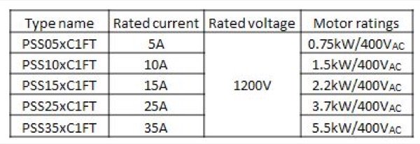
Table1: Motor ratings vs. DIPIPM+TM types
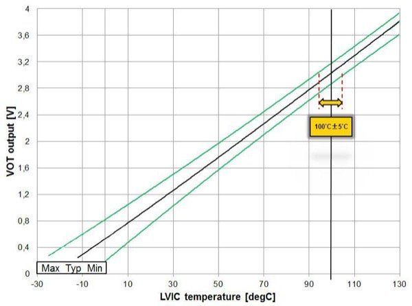
Figure 12: Analogue temperature output signal VOT from DIPIPM+TM
The analogue VOT-signal of DIPIPM+TM can also be used to increase the robustness of the inverter against harsh environmental conditions. Usually, the inverter specification is given for maximum ambient temperature of Ta=+40°C. For higher ambient temperatures an inverter de-rating has to be considered when installing the drive. By using the VOT-signal several options can be activated for an adaptive inverter de-rating during operation in case of reaching a critical device temperature before the over-temperature protection would turn-off the drive: for example by reducing the switching frequency fc or by reducing the inverter output current as a function of the VOT-signal.
Well suited for industrial inverter drives
The DIPIPM TM technology was originally developed for the needs of high volume inverterized white goods applications like washing machines, air-conditioners, refrigerators etc. Over the past 20 years more than 450Mio pieces DIPIPM have been manufactured by Mitsubishi Electric in different packages, voltage and current ratings [5]. For industrial drive applications usually 1200V DIPIPMs are being used. The new DIPIPM+TM series was developed for the specific needs of compact industrial 400VAC-inverters. It is compliant with Viso = AC2500V industrial isolation standards and meets all relevant industrial creepage and clearance requirements, see Figure 13.
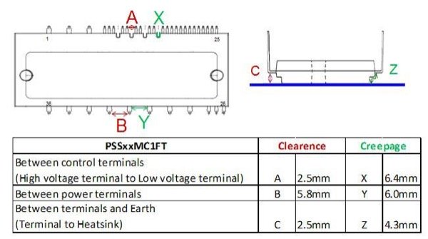
Figure 13: Creepage and clearance distances of DIPIPM+TM package
The DIPIPM+TM package is siloxane free and therefore well suited for applications where IGBT modules with silicone gel are not allowed. The DIPIPM+TM series is UL-approved (UL1557 File E323585) and ROHS compliant.
Summary
The new DIPIPM+TM series is an excellent answer to the needs of compact AC400V inverters in the power range between 0,75kW… 5,5kW. It helps to reduce both cost and size of a new inverter design. A plug-and-play evaluation board is available for shrinking the inverter development time. Based on 20-year experience with manufacturing of dual-in-line packaged IPMs for white good applications, with the new DIPIPM+TM series Mitsubishi Electric is now introducing an “all-in-one” DIPIPM-solution that meets all requirements of an industrial inverter design.
About Mitsubishi Electric
Mitsubishi Electric is one of the world’s leading companies in Manufacturing, Marketing and Sales of electric and electronic equipment used in communications, industrial technology, renewable energy and transportation.
References
- Mitsubishi Electric Corp.: “Mitsubishi Electric to launch DIPIPM+ Series” Press release No. 2928; May7, 2015
- M. Honsberg et al.: “A novel Transfer Molding Intelligent Convert Inverter Brake IGBT module (DIPIPM+) with integrated level shifting control ICs”, PCIM Europe 2016, Conference proceedings p.889-894
- Mitsubishi Electric Corp.: DIPIPM+ Evaluation Board User manual (Application Note dated 2015.07)
- Mitsubishi Electric Corp.: DIPIPM+ Series Application Note DPH12856 (publication date: July 2016)
- S. Noda et al.: “A novel Super Compact Intelligent Power Module”, PCIM Europe 1997, Conference proceedings p.1-9