Facebook
 Google
 GitHub
 Linkedin
Design Techniques for Lowering Noise in a Switch Mode Power Supply
Designing a circuit with switch mode power supplies (SMPS) can be daunting at first — especially when trying to mitigate noise. Deploying some of the techniques covered in this article can help improve simple reference design performance.
In the last article, we discussed the concept of noise (ripple and EMI) in an SMPS circuit, as well as the circuit’s layout and simple design techniques that can mitigate it. In this article, we will discuss noise from a larger system point of view. Placing multiple switch mode power supplies on one board can present new challenges, and we will discuss ways to design a power scheme such that these supplies do not interfere with one another.
Design and System Architecture
An SMPS isn’t designed to exist on its own. It’s a part of a larger system. The overall power architecture, based on available and required voltages, should be carefully assessed for the most efficient, cost-effective, and practical results.
For instance, say you have a 12V rail available and require a 3.3V rail for I/O, a 1.8V rail for RAM, and a 1.2V rail for a processor’s core supply. Instead of using three buck converters to achieve each desired output, you could choose to get a 3.3V rail from a buck converter with a greater current capability, and then generate 1.2V and 1.8V using linear regulators, with the 3.3V rail as their input.
Another option would be generating 3.3V through a buck converter, and then cascade LDOs to generate 1.8V from 3.3V, and 1.2V from 1.8V. The resulting circuit will likely be quieter in terms of ripple and EMI. While linear regulators are much less efficient than their switch-mode cousins, they do present advantages. They’re often cheaper, require less board space, and require fewer passive components around them to operate.
Linear regulators also have the ability to suppress the noise present on their input. This metric is called the power supply rejection ratio (PSRR), and it represents the ratio between the input voltage ripple and output voltage ripple, measured in decibels. Often, they’re around 40-60dB, but some may go up to 90dB or higher. A very sensitive net, such as for RAM or core voltage, have tighter voltage ripple requirements, and powering it through an LDO is a way to keep the ripple to a minimum.
When placing multiple SMPS on one circuit board, it can be beneficial to synchronize their clocks. An SMPS device typically controls the switching of its own internal MOSFETs while usually allowing a designer to select that switching frequency with an external component. However, some buck/boost devices come with a “SYNC” pin — a pin for an external clock signal.
The supplies should all use the same switching frequency, and the phase of the signals should be taken into consideration. This means that the supplies should all switch at the same time (fed the same clock signal, perhaps generated by a microcontroller), or should switch sequentially one after the other (generated with a multiphase oscillator, such as the LTC6902).

Figure 1. A 3-phase (120˚ phase shift between signals), 1 MHz clock signal, with a 33% duty cycle for each of the 3 phases, generated by the LTC6902
Selecting a switching frequency is one of the most important factors in designing a switch-mode power supply. This subject has already been covered many times, including in the article How to Choose the Frequency of Your Switching Regulator on All About Circuits.
In general, a higher switching frequency will lead to a lower magnitude voltage ripple. However, each circuit has an upper limit for how fast it can switch. This is dictated by the minimum on time, which is the shortest amount of time that the device can leave its switch closed.
Vout = ton(min) x VIn x FS(max) x η
Based on a known input voltage (VIn), a desired output voltage (Vout), efficiency (η), and minimum on time (ton(min)) from the datasheet, the device’s maximum switching frequency (FS(max)) for a given design can be calculated. For multiple switching regulators whose clocks will be synchronized, the switching frequency must not exceed the smallest calculated FS(max).
While it may not directly be related to EMI or voltage ripple, the location of the SMPS on a board can affect system performance. It is best to place switch mode power supplies as close to the voltage input as possible and to keep the supplies away from sensitive signals, such as high-speed digital signals (Ethernet and USB, for example), or analog signals (such as audio or analog sensors), which can be corrupted by the switching noise.
Some designers recommend using a “switching ground” (similar to the idea of an analog and digital ground), but separating grounds can cause problems for inexperienced designers. Proper design, layout, and location on the PCB can do just as good of a job.
Other Methods for Lowering SMPS Noise
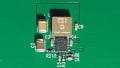
For circuits used in sensitive environments where there are other susceptible devices, or other devices generating EMI, it can be helpful to include an EMI shield on your PCB. This shield is as simple as a conductive metal box placed over sensitive or EMI-generating components. These shields can be purchased off-the-shelf, with the layout designed around it, or custom-designed (either in large quantities or handmade from metal sheets cut and folded to size).

Figure 2. EMI Shield. Image courtesy of Harwin.
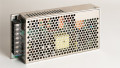
There are also many off-the-shelf SMPS solutions that can be deployed on a custom PCB. These modules can save board space and design complexity at the trade-off of a higher price.

Figure 3. Murata OKL2-T/20-W12N2-C. Image courtesy of Digikey.
Designing a circuit with switch mode power supplies can be daunting at first, but the benefits by far outweigh the complexity in the right application. Tools like TI’s Webench Power Designer can simplify the process. But by deploying some of the described techniques, a simple reference design’s performance can be greatly improved.