Facebook
 Google
 GitHub
 Linkedin
Analog Electronics Basics: An Overview of BiCMOS Operational Amplifiers
Learn about the operational amplifier, a device employed to perform a broad range of linear functions.
Operational amplifiers (op-amps) are by far the most versatile of the linear ICs. These are “operational” amplifiers since they initially performed mathematical operations. Op-amps amplify the difference between voltages or signals applied to their two inputs. The voltage applied to one input will only be amplified if the second input is grounded or held at some voltage level.
The BiCMOS Logic Family
The BiCMOS logic family integrates bipolar and CMOS devices on a single chip to combine the advantages of both families. The bipolar logic families have higher switching speeds, and higher output drive current capacity. The CMOS family has lower power dissipation, better noise margin, and higher packing density.
The Operational Amplifier
The operational amplifier (op-amp) is a high gain voltage-controlled voltage source (VCVS) with differential inputs and one output.
The initial op-amps employed thermionic tubes polarized at high voltages to electrically perform, in analog computers, mathematical operations such as addition, subtraction, multiplication, division, integration, derivation, and others. Hence its name of an operational amplifier. Although its use has spread to many applications outside of analog computing, it keeps this name.
Currently, they are integrated circuits with several encapsulations, low working potentials, reliable, inexpensive, and may employ a single power supply.
Figure 1 shows the general symbol of the op-amp.
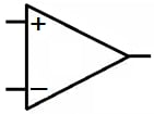
Figure 1. The circuit symbol of the op-amp.
Figure 2 shows the currents and voltages in the op-amp.
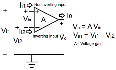
Figure 2. Current and voltages in the op-amp.
Node voltages referenced to ground. The input with a plus sign is the noninverting input, and the input with a negative symbol is the inverting input. The op-amp symbol does not always show the ground, but it is there at all times.
Typically, circuit diagrams omit power supplies – required for the op-amp to operate – for clarity.
The input voltage Vin = Vi1 – Vi2. As a dependent source, the op-amp amplifies the input voltage. In figure 2, the open-loop gain of the op-amp (A) dictates the degree of input voltage amplification – defined as the ratio Vo/Vin.
Amplifiers with a single input are a particular case, with one input grounded.
The op-amp may be found as integrated circuits or discrete components with an extraordinary number of functions.
The Ideal Operational Amplifier
The ideal op-amp responds only to the voltage difference between the two inputs. The op-amp without feedback is said to work in open-loop mode – its feedback circuit is not closed.
The ideal op-amp has infinite voltage gain, input impedance, and bandwidth, zero output impedance, zero response time, and no noise. Since the input impedance is infinite, the input currents are also zero.
Summarizing:
Voltage gain = ∞
Input impedance = ∞
Bandwidth = ∞
Output impedance = 0
Perfect balance: Vo = 0 when V2 = V1.
These characteristics are independent of temperature.
The Real Operational Amplifier
An ideal op-amp has infinite input impedance and draws no current from the source – and thus no power. This device is not realistic because any amplifier must draw some power from the source to sense the signal to amplify.
Real op-amps can’t meet the ideal open-loop characteristics. Instead, they seek those ideal parameters.
Real op-amps have voltage gains ranging from 10³ (60 dB) to 10⁹ (180 dB), typically 10⁵ (100 dB), and a flat response - constant gain - from 0 Hz to several kilohertz.
The input impedance spans from 10⁵ to 10¹² ohms, and the output impedance from 25 to 50 ohms. Since op-amps do not have infinite input impedance, their input current is not zero. This small current creates an offset voltage at the output that can be partially compensated by a resistor Rc as shown in figures 5 and 6.
The actual parameters depend on the particular op-amp model. The numbers mentioned above are referential. In practice, it is mandatory to use the parameters specified in the manufacturer’s datasheet.
Open-loop operation
The op-amp has an inverting and a noninverting input. The polarity at the output reverses the polarity of the input voltage when applied to the inverting input. The output polarity is the same when applied to the noninverting input. Figures 3 and 4 show both modes of operation.
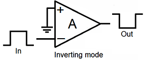
Figure 3. Inverting mode operation.
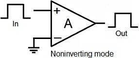
Figure 4. Non Inverting mode operation.
These settings allow the op-amp to operate at its maximum voltage gain level.
As seen in figure 2, with no feedback, the output of the op-amp equals the potential difference at its two inputs times the voltage gain. As indicated above, the voltage gain of an ideal device is infinite.
Assuming an actual device with a voltage gain of 10⁵ and 1 V input, the output should be 100 kV. However, the output voltage cannot exceed the highest power source voltage to avoid saturation.
We see that the high gain of the open-loop configuration makes the amplifier unstable because even small input signals may generate saturation. For this reason, the open-loop layout is not practical. The connection of a feedback circuit – closed-loop operation – solves this instability problem, despite losing part of the gain.
Closed-loop operation
We see that the op-amp is very valuable as a general-purpose amplifier mainly due to its high gain.
The main difference between an operational amplifier and an ordinary differential amplifier is that the former utilizes external feedback networks – a part of the output signal is fed back to the input via several paths, depending on the specific function required.
The gain in closed-loop circuits differs from that in open-loop circuits – which is the voltage gain A. It is helpful to use external feedback connections so that the overall voltage gain or characteristics of the amplifier output signal depend mainly on the parameters of the elements in the feedback circuit.
Typical passive electrical components used in the feedback circuit have stable and exactly known values. This format controls the overall output characteristics of the op-amp, independent of the properties of the amplifier element itself. Connecting the feedback circuit to the basic op-amp makes it work in closed-loop mode.
The two basic closed-loop amplification circuits are the inverting amplifier (figure 5) and the noninverting amplifier (figure 6).
The Inverting Amplifier
The inverting amplifier incorporates negative feedback connecting an external resistor Rf between the output and the negative – inverting – input.
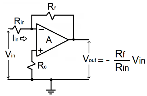
Figure 5. Closed-loop inverting amplifier.
Under this state, the input voltage to the negative terminal is Vin plus the feedback voltage. The input resistor Rin separates these two voltages. The input resistance of a real amplifier is equal to Rin.
Assuming an ideal op-amp and defining the closed-loop gain as
G = Vout/Vin
The inverting amplifier has a closed-loop gain of
G = −Rf/Rin
The gain of the inverting amplifier will always be negative, whence its mane.
Although negative feedback accurately controls the whole voltage gain of the amplifier, it reduces its magnitude. The designer's choice of Rin and Rf will set the absolute gain independently of the open-loop gain A.
The equation in figure 5 shows that the output voltage is negative (provided Vin > 0).
The previous equations show that Vout = G Vin, so the output voltage is linear.
The Noninverting Amplifier
A solution to amplify without sign change is the noninverting amplifier configuration, shown in figure 6. The input voltage feeds the positive input, and the output voltage becomes positive, in contrast with the inverting amplifier – now, the output voltage keeps the input polarity.
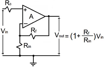
Figure 6. Closed-loop non inverting amplifier.
Applying part of the output voltage back to the negative or inverting terminal – through a voltage divider network – provides feedback control.
Again, assuming an ideal op-amp and defining the closed-loop gain as
G = Vout/Vin
The noninverting amplifier has a closed-loop gain of
G = 1 + (Rf/Rin)
Looking at some particular values, note that if Rf = 0, the voltage gain will be one. If Rin = 0, the gain, theoretically, will approach infinity, but in practice, it will be the open-loop gain A. The voltage gain will never be less than one for passive resistors with nonnegative resistance.
Detailed circuit analysis of the non inverting configuration shows that the gain G has an additional 1/A term, involving the open-loop gain. For practical purposes, this term is zero, considering the high value of A.
The non inverting configuration features minimal gain and high input impedance characteristics.
The Voltage Follower
The name voltage follower comes from the fact that the output voltage is equal in sign and magnitude to the input voltage. The voltage follower takes advantage of the non inverting configuration’s low gain, high input impedance, and low output impedance.
In negative feedback systems, we have seen that the output is subtracted from the input – by connecting the output terminal to the inverting input. Making Rf = 0, Rin = infinite, and neglecting Rc, in the noninverting amplifier of figure 6, we get the circuit shown in figure 7.
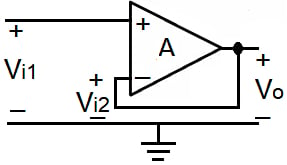
Figure 7. Voltage follower.
The connection of the input voltage directly to the non inverting input of the op-amp, results in the output and input voltages being in phase.
The voltages at the two op-amp inputs, Vi1 and Vi2, must be precisely the same. If the voltage Vi1 rises, the output voltage Vo also rises. Since there is feedback between the output and the negative terminal, Vi2 increases by the same amount.
Since Vin = Vi1 - Vi2, Vi2 reduces the voltage between the two inputs, decreasing Vo. The process soon stabilizes, and Vo remains at the value needed to keep the two inputs ideally identical. This result is an unmistakable sign of negative feedback.
It may be shown that the gain Vo/Vi1 in figure 7 is A/(A+1). For significant gains, this ratio is close to 1. This means that the output voltage Vo follows the input voltage Vi1 without amplification or any other change.
In contrast, recall that, without feedback, Vo/Vin = A.
The voltage follower isolates the output from the input. It is helpful when impedance matching or circuit isolation is essential. An example of employing its high input impedance is when used at the input of a measuring instrument to take shallow currents from the measured circuit.
A Physical Operational Amplifier
A mechanism intended to perform a simple task as a high gain voltage-controlled voltage source is a very complex circuit.
A physical op-amp is an involved arrangement of transistors, resistors, diodes, and other elements. As an illustration, figure 8 shows a simplified schematic of a Renesas CA3130 op-amp (15MHz, BiMOS Operational Amplifier with MOSFET Input/CMOS Output).
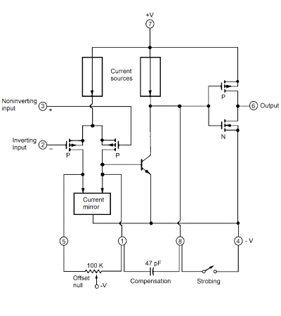
Figure 8. Simplified schematic diagram of a CA3130 BiMOS op-amp.
The CA3130 has an inverting input (pin 2) and a noninverting input (pin 3). These inputs supply the gates of two p-channel field-effect transistors working as a differential amplifier. This fact provides a very high input impedance, which translates into a tiny input loading in most cases.
Differences in voltage between the two inputs proportionally split the current from the upper current source, sending a fraction of the current through each transistor. A particular circuit – the current mirror – senses current imbalances in the transistors. The current mirror also works as a differential-to-single-ended converter.
The single-ended current unbalance is amplified and goes to a second amplifier stage – a single NPN bipolar transistor. The second amplifier stage provides most of the op-amp voltage gain.
The second stage drives a push-pull output stage similar to a CMOS inverter operating as a Class-A amplifier. This output stage is a drain-loaded amplifier, and its gain depends upon the load impedance.
The three gain stages amplify any voltage difference on the non inverting and inverting inputs and output on pin 6. A voltage increase on the noninverting input drives the output positive. A voltage increase on the inverting input forces the output negative.
Operational amplifiers have an inherent input offset voltage – the voltage that must be applied between the two input terminals to get an output of zero volts. The offset-null potentiometer between pins 5 and 1 unbalances the current mirror and compensates for the input offset voltage. This potentiometer may have a value of 100 kΩ with the slider arm connected to pin 4.
A single external capacitor, between pins 1 and 8, will phase compensate for the op-amp. It means a reduction of the high-frequency response to remain stable. A 47pF capacitor will do in most applications.
For strobing – to gain digital control over the presence or absence of a signal – you connect pin 8 to pin 4 (negative supply). This connection forces the output (pin 6) to the positive supply (pin 7) and minimizes the current employed by the output stage.
Pin 8 is also helpful for phase compensation.
About BiCMOS Op-Amps
The BiMOS logic family uses both bipolar and MOS devices.
The operational amplifier is a significant building block in Electronics.
Early op-amps used discrete components, like vacuum tubes. Their initial applications were analog computation and instrumentation. Today, op-amps are very versatile, with many applications.
The op-amp has two inputs and one output. The symbol of the op-amp does not always show the power supplies for simplicity.
The ideal op-amp senses the difference between the voltages applied at its two inputs and multiplies this by the voltage gain A, producing an output voltage of Vo = A Vin.
The input impedance of an ideal op-amp is infinite, and it does not draw any input current. The output impedance is zero, independently of the load current.
The value of the voltage gain A is substantial and ideally infinite.
Physical IC op-amp characteristics approach those of the ideal device.
The input terminal distinguished by a negative sign is the inverting input. The input terminal indicated by a positive symbol is the noninverting input.
The output voltage is in phase with the voltage applied at the noninverting input and out of phase with the voltage applied to the inverting input.
Usually, the open-loop configuration is not practical. More common is the closed-loop design with passive components in a feedback circuit.
The two closed-loop configurations are inverting and noninverting.
In a voltage follower, the output “follows” the input.
Physical IC op-amps components are transistors, resistors, and diodes connected in complex networks.