Facebook
 Google
 GitHub
 Linkedin
Power Modules for Onboard Chargers
Electric vehicles are fast becoming state-of-the-art. Modern EVs can cover distances between 400 to 600 km on a single charge due to increased Li-ion battery capacity, elevated nominal battery voltage, and wide bandgap semiconductors.
To accommodate the full potential of this increased battery capacity, high-speed charging becomes inevitable. For AC charging in passenger cars, onboard chargers (OBCs) are required. Earlier, the most common power rating of OBCs was in the range of 3.6 kW to 7.2 kW. However, with an increase in the battery capacity, the popularity of OBCs with rated powers of 11 kW and 22 kW will also increase.
Increased power rating and production volumes pose some challenges for modern OBC designs. For instance, despite the fact that the power rating of OBCs increases, the available installation space for the OBC stays nearly unchanged due to the limited space in EVs. Therefore, an OBC with an 11 kW or higher power rating will require a higher power density (W/l) compared to former OBC solutions. Additionally, as the power density of an OBC increases, the cooling of semiconductors in the OBC also becomes more crucial. This makes an optimized thermal connection between the semiconductors to the heatsink essential.
Another challenge that modern OBCs need to address is fast and robust manufacturing. To meet the increasing production demands, OBCs need to be designed such that their production can be realized through automation. Additionally, to reduce costs at the system level, vertical integration of components, for example, in the form of power semiconductor modules, is also required. In short, to meet the increasing demand for EVs equipped with OBCs of 11 kW or higher charging power, design and manufacturing processes need to be optimized.

Figure 1. EasyPACK family with AQG324 qualification for OBCs. Image used courtesy of Bodo’s Power Systems [PDF]
As one of the industrial module standards set by Infineon Technologies, EasyPACK modules are used in applications such as EV chargers, general-purpose drives, solar inverters, air conditioners, and many more. The two sizes of EasyPACK modules with AQG324 qualification, as shown in Figure 1, provide the optimal area required for the semiconductors to realize a compact OBC solution.
A typical OBC consists mainly of a power factor correction (PFC) stage and the primary and secondary sides of a DC/DC converter. For example, a 22 kW OBC solution can be easily achieved by using EasyPACK 2B and EasyPACK1 B. The EasyPACK 2B can utilize, for example, 12 pieces of 33 mOhm 1200 V CoolSiC M1H MOSFETs, allowing the PFC stage and the primary side of the DC/ DC to be realized, as shown in Figure 2 (a). Additionally, a negative temperature coefficient (NTC) resistance can be integrated into the module to monitor its internal temperature. On the secondary side of the DC/DC converter, the EasyPACK 1B can accommodate four pieces of 33 mOhm 1200 V CoolSiC M1H MOSFETs. However, EasyPACK 1B offers enough area to house the primary side of a high voltage to low voltage (HV/LV) DC/DC converter as well as an NTC, as shown in Figure 2 (b). Using EasyPACK 2B and EasyPACK 1B, the area required for semiconductor switches of a 22 kW OBC on the heat sink can be reduced to 43.4 cm². This design not only enables a high power density but also reduces the heat sink area providing more design flexibility.

Figure 2. Common topology of OBC consisting of PFC (a) The primary side of DC/DC converter (b) The secondary side of DC/DC converter with integrated primary side of HV/LV DC/DC converter. Image used courtesy of Bodo’s Power Systems [PDF]
The semiconductors in EasyPACK modules are placed on a direct bonded copper (DBC) substrate. The layers of the DBC are shown in Figure 3. On the top copper layer, the semiconductors are connected via soldering and wire bonding. The ceramic material between the top and bottom layer (can be either Al2O3, AlN, or Si3N4) isolates the high potential of the semiconductors from the ground. This eliminates the necessity of an additional isolation layer for the power semiconductors, which is an additional leverage for reducing the bill of materials and processing steps in production. One additional benefit of the DBC substrate, thanks to the ceramic layer, is stable isolation properties over its lifetime.

Figure 3. Cross sections of the PressFIT contact zones [2]. Image used courtesy of Bodo’s Power Systems [PDF]
The connection of EasyPACK modules to the printed circuit board (PCB) is realized by PressFIT pins. The PressFIT pin has a press zone with galvanized tin that forms a cold-welding contact with FR4 PCBs. A cross-section of welded parts is shown in Figure 4. This interconnection provides consistent and continuous low electrical contact resistance (as low as 0.05 mOhm [1]). The cold-welded PressFIT contacts offer a very low failure-in-time (FIT) rate that, according to [2], is a factor of six lower than that of automated soldered contacts.

Figure 4. The layers of a DBC in an EasyPACK. Image used courtesy of Bodo’s Power Systems [PDF]
Another benefit of PressFIT pins is the reduction in production complexity compared to selective soldering. Due to the height of the passive components and modules that need to be connected to the heat sink, the modules are located on the opposite side of the contact pins of the through-hole components. As the pins are pressed, only the side of the PCB, on which the contacts of through-hole components, such as capacitors, connectors, and transformers, are placed, must be selectively soldered. Using the PressFIT pins to contact the modules to PCB, therefore, reduces processing time and handling complexity; thereby reducing production costs.

Figure 5. The construction of EasyPACK allows a low cavity between the module and heatsink. Image used courtesy of Bodo’s Power Systems [PDF]
Another characteristic of EasyPACK is its very good thermal performance. EasyPACK modules are screwed directly onto the heat sink (see Figure 5). This construction of the EasyPACK modules allows them to be fixed to the heat sink with a very low cavity. The resulting thickness of the thermal interface material (TIM) layer between the bottom side of the DBC and the heatsink is less than 100 µm. Such a thin TIM layer is sufficient to fill up the cavity and assure the connection of semiconductors with very low thermal resistance to the heat sink. For instance, an 80 mOhm 1200 V CoolSIC M1H in EasyPACK can achieve power losses of up to 30 W without exceeding the Tvj,max.
Furthermore, the screwed EasyPACK in combination with PressFIT pins eliminates nearly all mechanical and assembly process-related tolerances and reduces the mechanical stress on the PCB.
Growing Demand for Onboard Chargers
The growing demand for OBCs with higher power ratings, such as 11 kW and 22 kW, necessitates higher vertical integration and easier manufacturing capability to increase productivity and achieve better economies of scale. These requirements can be easily fulfilled by using integrated power modules such as EasyPACK. For example, it is possible to concentrate power semiconductors in an 800 V 22 kW OBC within a 43.4 cm² area using a single EasyPACK 2B for the PFC stage and primary side of the DC/DC, and a single EasyPACK 1B for the secondary side of the DC/DC. The utilization of EasyPACK 1B for the secondary DC/DC stage can be further extended by integrating an H-bridge as the primary side of an HV/LV DC/DC converter to bring the power density for combined systems to an even higher level.
High power density, integrated isolation, fast and robust manufacturing capability, and lower FIT rate due to PressFIT pins make the existing EasyPACK module family with AQG324 qualification an excellent solution to meet the demands of OBCs with 11 kW and above power rating.
References
[1] AN-Automotive EasyPACK-Assembly, revision 1.0, 7 Sept. 2021
[2] Siemens norm SN 29500-5/Edition 2004–06
This article originally appeared in Bodo’s Power Systems [PDF] magazine and is co-authored by Koray Yilmaz and Christoph Schäfer of Infineon Technologies.
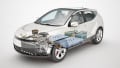
Featured image used courtesy of Adobe Stock