Current Source Gate Drivers Boost the Turn-On Performance of IGBT
This article highlights Infineon 1EDS20I12SV and a conventional gate driver IC, which gate drivers are operated by FF1200R12IE5 1200A/1200V power module.
Design engineers for gate drive are oftentimes required to employ turn-ON resistors that are bigger than the suggested capacity of the datasheet for IGBT, making the dvCE/dt slow down during current commutation. Infineon Technologies offers the 1EDS20I12SV, a new gate driver IC that controls a relatively constant dvCE/dt.
This article shows a comparison of two gate drivers: Infineon’s 1EDS20I12SV and a conventional gate driver IC. Both gate drivers are operated by the FF1200R12IE5, a 1200A/1200V power module intended for high power applications. This comparison unveils the advantages of the new control method.
The IGBT's Control Equations
It is helpful for the understanding of the control scheme of 1EDS20I12SV to analyze the turn-ON behavior of an IGBT as it is depicted in Figure 1 for an inductive load. For simplicity, the commutating diode is a SiC Schottky diode for which reverse recovery is purely capacitive.
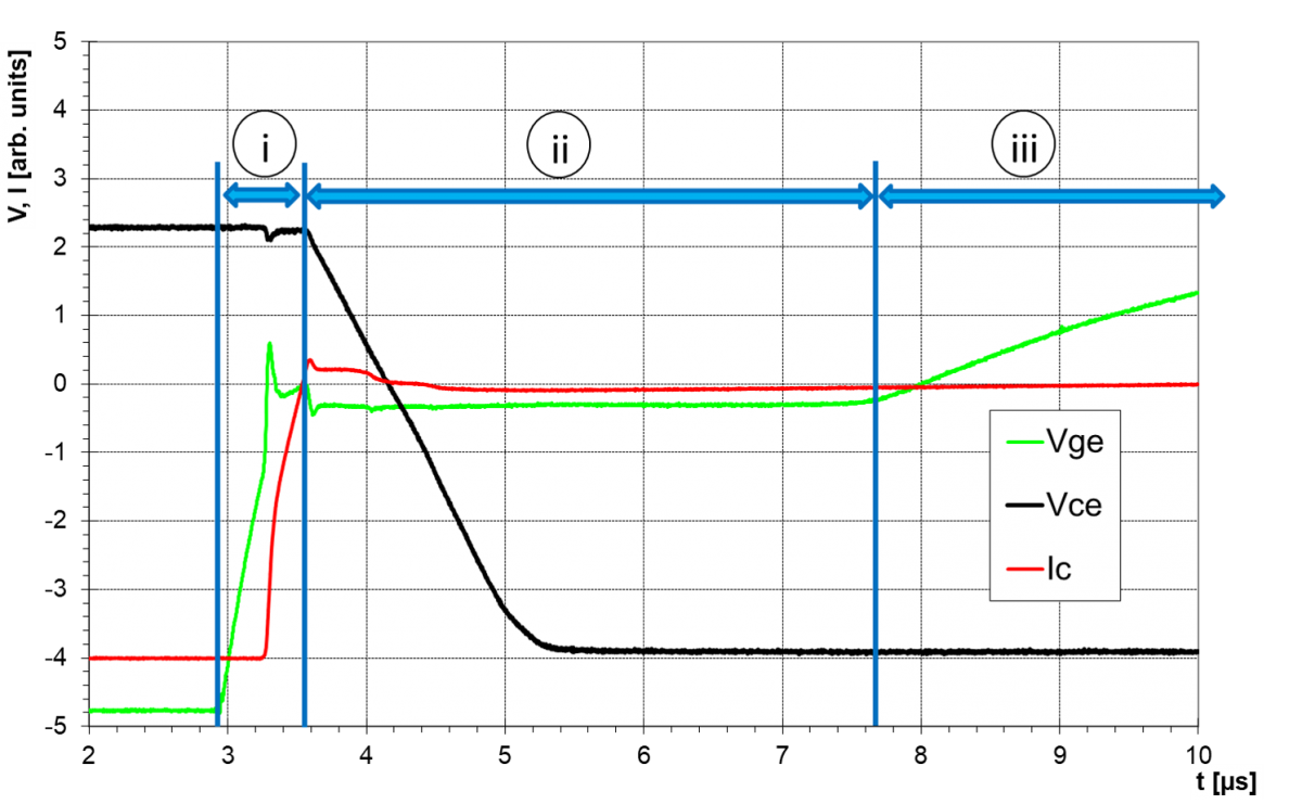
Figure 1. Typical turn-ON transient of an IGBT divided into 3 sections.
The IGBT's Control Equations
It is helpful for the understanding of the control scheme of 1EDS20I12SV to analyze the turn-on behavior of an IGBT as it is depicted in Figure 1 for an inductive load. For simplicity, the commutating diode is a SiC Schottky diode for which reverse recovery is purely capacitive.
The gate current Ig charges both the gate emitter capacitance Cgeand the gate collector capacitance C g caccording to [4], [5]:
The gate-emitter capacitance can be assumed to be voltage-independent, whereas the voltage dependency of Cgc is significant. The capacity Cgc is low at large values of Vgc but large for small voltages.
Note that the gate-collector voltage is given by
In a simplified picture, the turn-ON of the IGBT can then be divided into three phases:
- Gate charging at high Vce: first term of eq. (5) dominates
- Miller plateau at constant Vge and changing Vce: second term of eq. (5) dominates
- Gate charging at low Vce: first term of eq. (5) dominates again
The difference between voltage driving and current driving schemes then becomes obvious.
For a voltage driving scheme, the gate current is changing during the switching transition according to
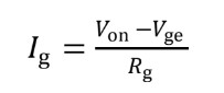
Where Von is the voltage supplied by the gate driving circuit.
dVce/dt during phase (ii) and therefore the turn-ON energy Eon is then determined by the Miller voltage which in turn depends on the load current. Low currents and comparatively low Miller voltages will result in high dVce/dt during turn-ON.
On the other hand, the turn-ON energy Eon when handling larger collector currents is increased both by the higher current level itself and the slower switching speed due to the high Miller voltages and associated lower gate currents. This results in non-linear curves for the turn-ON energy as a function of the collector current.
The choice of gate resistors is determined by the need to limit the voltage slope at small currents. This is detrimental for the losses when switching high currents.
With a gate current driving scheme, the dVce/dt during phase (ii) is independent of the load current, thus allowing optimized switching speed for a wide current range. The turn-ON energy is therefore only depending on the collector current amplitude at turn-ON.
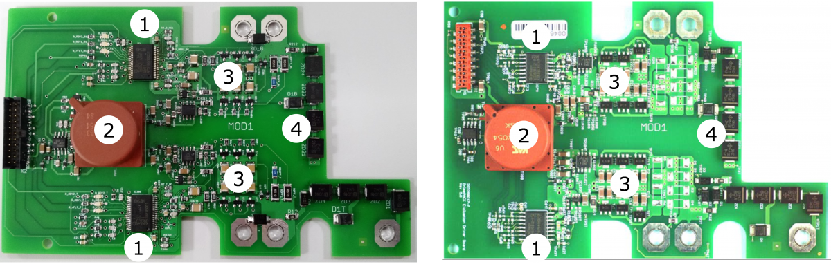
Figure 2. Driver board with current source gate control (left) and voltage source gate control (right).
Gate Driver Boards
Both driver boards are designed to fit the power module FF1200R12IE5. They contain external buffers (3), which amplify the driver IC s (1) output current. The buffer of the conventional realization (left in Figure 2) is based on bipolar transistors, while the current source gate driver board used p-channel MOSFETs for boosting the turn-ON.
The use of p-channel MOSFETs is mandatory for the gate current control loop. The turn-OFF boost circuit uses pnp-transistors similar to the conventional gate driver board. An output bias supply (2) provides the gate drive voltages for a +15 V / -8 V supply.
Finally, there is also an active clamping function (4), which acts on the gate voltage to avoid overvoltages during turn-OFF. Since the active clamping is only activated during turn-OFF, it does not interfere with the constant current turn-on.
The current source gate driver IC contains the option to change the switching speed pulse-by-pulse during operation. This is an important function to reduce the turn-ON switching losses furthermore in the application [1].
Gate Current Control Turn-ON Scheme
The first phase during turn-ON is the preboost phase and lasts for 135ns according to Figure 3. The preboost charges the gate-emitter voltage to a value below the gate-emitter threshold voltage Vge(th). The current during the preboost phase depends on the gate charge and is therefore constant throughout the operation of a given power switch.
The turn-ON phase follows the preboost. The turn-ON current level can be selected arbitrarily during operation out of 11 levels. The selected gate current level yields in a given turn-ON speed.
The selection of the switching speed levels is done by applying an analog signal to a specific terminal on the control side of the gate driver IC. The turn-ON current level is active until the gate reaches the final gate bias voltage, which is 15 V in this case.
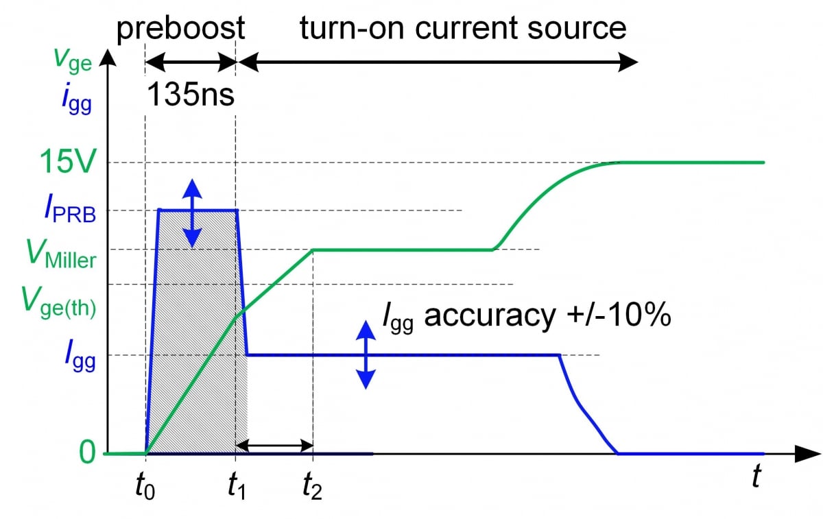
Figure 3: Turn-ON sequence of the current source gate driver IC 1EDS20I12SV.
Measurement Results
Both gate driver systems are evaluated on a double pulse test bench with automated switching parameter calculation. The double pulse technique is explained elsewhere. The boards are operated with various turn-ON speeds in order to evaluate as well the trend of each parameter as a function of the switching speed. This is achieved by using the integrated speed selection option of the current source gate driver IC and by variation of gate resistors of the conventional voltage source gate driver board.
Figure 4 shows an example of turn-ON waveforms. The gate-emitter voltage vGE (green) and the collector current iC (red) are smooth with acceptable small oscillations. The voltage slew rate dvCE/dt is evaluated shortly after the reverse recovery of the freewheeling diode (instance “1”). The diode takes over the voltage from the IGBT there and there is in many cases the largest dvCE/dt. Therefore, Figure 5 shows the transient of the diode ́s reverse voltage.
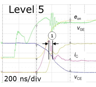
Figure 4: Example waveforms for turn-ON at IC = 120 A (10% of nominal current) and DC-link voltage of VDC= 600 V
Figure 5 depicts the results and contains marks which designate the design point of the gate drive in order to keep the dvR/dt at 5 V/ns or below.
This is in case of the current source solution the curve representing “level 5” and the curve of RG = 2.2 Ω for the voltage source solution. It can be seen that the dvR/dt stays relatively constant for the constant current source gate driver board because the gate current is constant over the whole turn-ON-process regardless of the individual collector current.
This yields in a constant dvR/dt. This is different for the voltage source board. The dvR/dt is constantly decreasing there, because the increasing miller voltage over the collector current range reduces the driving voltage for the gate current, and thus the gate current itself.

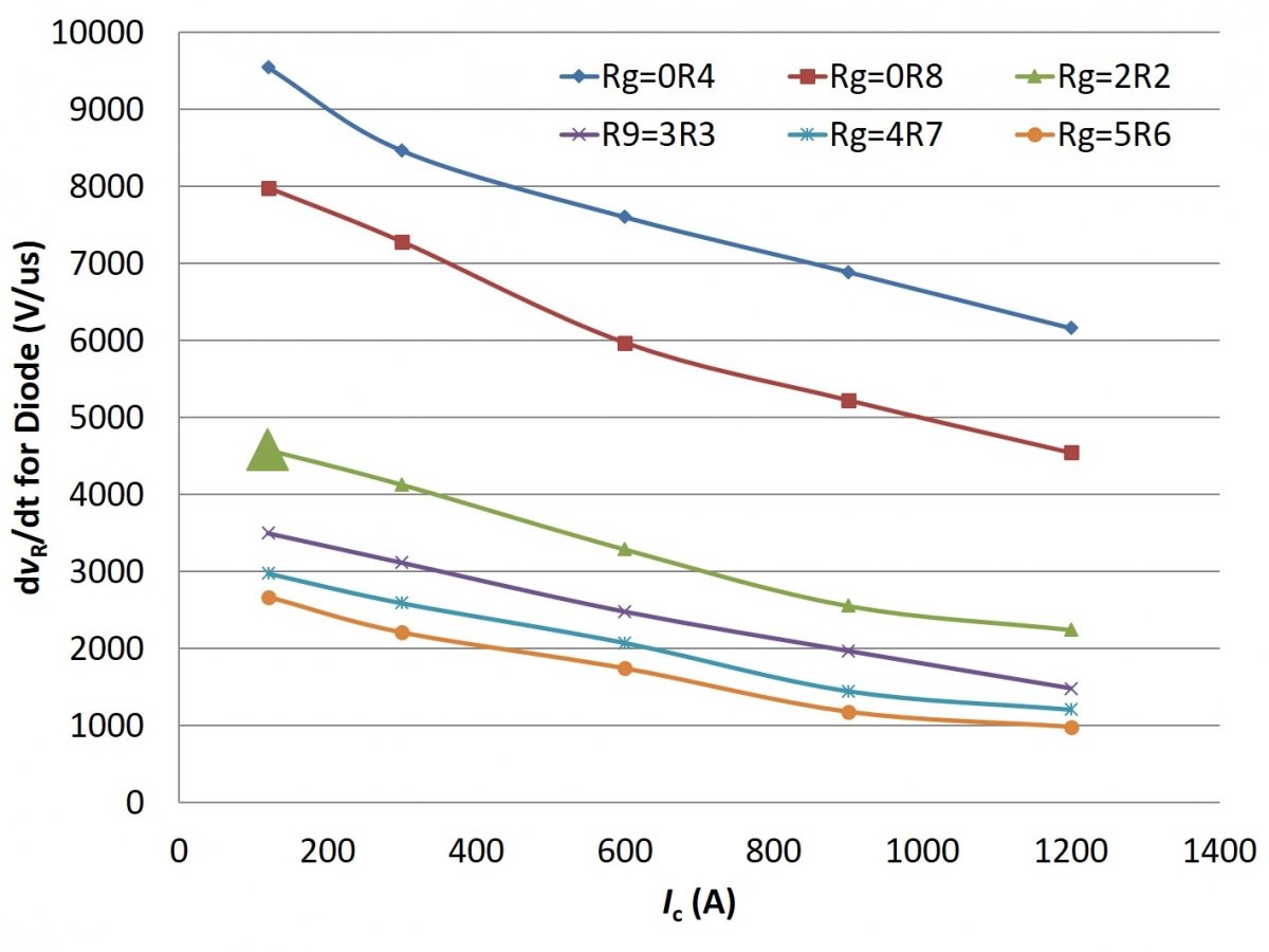
Figure 5. dvR/dt of the measured power module with current source gate control (top) and voltage source gate control (bottom).
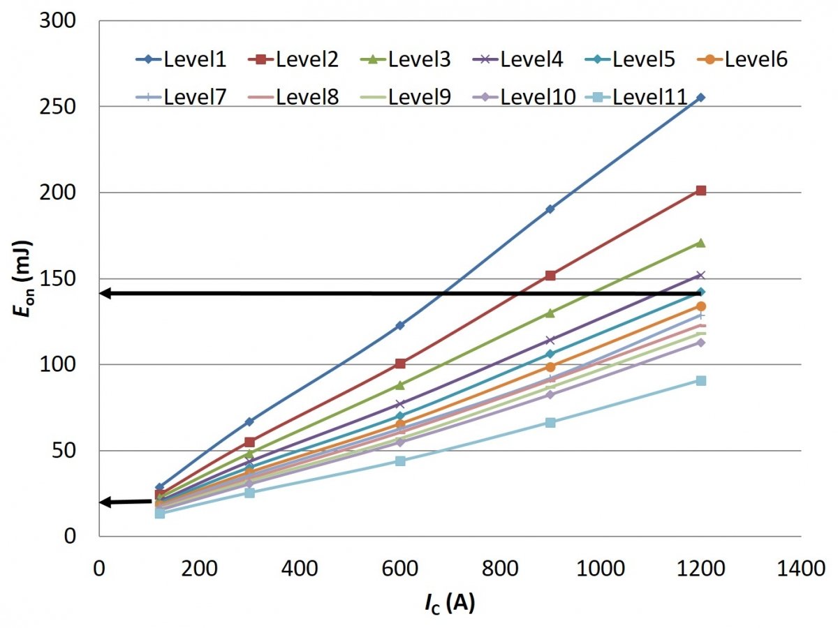
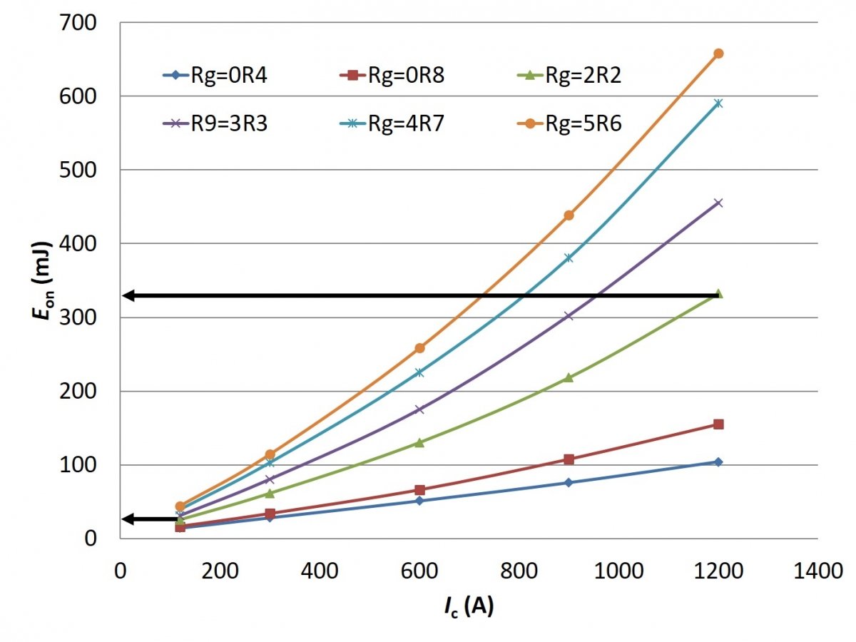
Figure 6: Turn-ON energy of FF1200R12IE5 measured with current source gate control with a change of switching speed (top) and voltage source gate control (bottom).
Figure 6 represents the turn-ON energy Eon of both solutions. The same starting conditions at 5 V/ns indicate also similar turn-on energy, which is approximately 20 mJ. However, the situation changes at high collector currents.
Here, the constant gate current source yields in a turn-ON energy of only 140 mJ compared to the voltage source driver board with approximately 340 mJ. Thus, the turn-ON energy of the constant gate current driver is only 41 percent of the voltage source gate driver solution at the rated collector current.
Conclusion
The gate current source turn-ON shows much lower turn-ON energy at similar dvCE/dt compared to voltage source gate drivers over the rated collector current range. Therefore, the current source gate control board is superior to conventional voltage source gate driver systems, which operate with a fixed turn-ON gate resistor.
A higher performing system can be achieved at a competitive cost compared to a conventional system. The adjustment of switching speed during operation results in a new degree of freedom for the gate current gate driver because it can adapt the turn-ON with respect to other operating conditions, such as the IGBT temperature or the load condition. [6] This advantage translates of course into larger temperature margins or output current margins on a system level, as well.
References
[1] W. Frank, et al.: Real-time adjustable gate current control IC solves dv/dt problems in electric drives, Proceedings of PCIM 2014, Nuremberg, Germany, 2014.
[2] Infineon: 1ED020I12-F2, datasheet, Infineon Technologies AG, Germany.
[3] Infineon: 1EDS20I12SV, datasheet, Infineon Technologies AG, Germany.
[4] J. Lutz, Semiconductor Power Devices, Springer Verlag Berlin Heidelberg, 2011, ISBN 3-540-34206-0.
[5] D. Schröder, Leistungselektronische Bauelemente, Springer Verlag Berlin Heidelberg, 2nd Edition, ISBN 3-540-28728-0.
[6] S. Mahmodicherati, N. Ganesan, L. Ravi, R. Tallam: Application of Active Gate Driver in Variable Frequency Drives; Proceedings of 10th IEEE-ECCE Conference; Portland, USA, 2018
About the Authors
Wolfgang Frank is the principal engineer for product definition and concept of gate driver ICs at Infineon Technologies. Earning his degree in power engineering from Technical University, Munich, he has worked in power engineering for over 20 years.
Holger Hüsken works for Infineon Technologies. He has authored a variety of articles centered around power engineering, particularly high-speed IGBTs. He is the co-owner of patents centering on semiconductor device technology.