Facebook
 Google
 GitHub
 Linkedin
Providing ESD Protection Through the Right Device Selection
ESD transients can occur anytime. As digital signal speeds increase and supply voltage rails reduce, selecting the right protection becomes even more important.
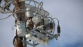
Analysts predict that tens of billions of connected electronic devices will come online over the next few years, as part of the expansion of the internet of things (IoT). It is safe to assume that the total number of electronic devices in general use is even higher. Many of these devices will perform important roles in our lives, such as consumer devices for home automation. Others might be embedded deeply and hidden from view, such as inside vehicles and smart buildings. All of them will be susceptible to electrostatic discharge (ESD). As the IoT connects more things to make networks of networks, any part of these billions of devices could become critical. This puts even greater emphasis on the design in the right level of ESD protection.
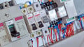
It is reasonable to say that, even after a printed circuit board (PCB) is assembled and installed in a device, ESD remains one of the main causes of failure. Modern integrated devices are designed to be robust, with little chance of functional faults occurring in the field. Operational conditions will, therefore, be the biggest challenge. While engineers can design for environmental extremes such as humidity, temperature, and vibration, ESD remains largely unpredictable. The best approach is to design adequate protection against the introduction of an electrostatic discharge.
In terms of testing that protection, standards such as IEC 61000-4-2 define levels of protection based on the severity of the discharge voltage used for test purposes. For example, Level 1 of the standard is defined as ± 2 kV for contact discharge and ± 2 kV for air discharge, while Level 4 specifies ± 8 kV for contact discharge and ± 15 kV for air discharge. The method of discharge and the shape of the transient used for testing is also closely defined, to provide repeatable evidence. The human-body model is widely used for testing purposes and is defined by standards such as MIL-STD-883 and JEDEC JS-001.
The Effects of ESD on Electronic Devices
The yellow and black warning symbols used by manufacturers to identify electrostatic-sensitive devices are commonplace in the industry. Integrated circuits (ICs), based on a metal oxide process to form transistors with insulated gates, are well known for their sensitivity. It is also important to appreciate that as supply rail voltages come down (one technique widely adopted to reduce active power), it also has the effect of lowering what little inherent protection from ESD that the devices might have.
Almost all general-purpose ICs are now based on metal-oxide-semiconductor field-effect transistors (MOSFETs), and many have supply voltage rails that are 1 V or lower. This makes them more susceptible to the transient effects of ESD. Exposure to high voltages and instantaneous currents present in a discharge can destroy parts of an IC immediately or cause low levels of damage that effectively shorten its working lifetime. This variability in severity only increases the difficulty of assessing the health of integrated circuits.
Transients can dissipate quickly without causing any damage or cause interconnects to fuse together resulting in irreparable damage. The nature of the substrate, lead frame, and packaging make it difficult to build adequate levels of ESD protection. The protection must be provided externally and positioned to arrest discharge as it happens. This generally means placing protection as physically close to the vulnerability as possible.
As design practices change it is important to appreciate how these evolving features can influence the type of protection selected. In many situations the design choice is wide, but some design features, such as high-speed serial buses, will limit the efficacy or applicability of some ESD devices. Parameters such as insertion loss and breakdown voltage must be assessed against the characteristics of the signals being protected in order to remain within functional envelopes.
Understanding ESD Protection Devices
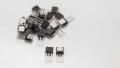
In general, ESD protection devices are either semiconductor-based in the form of transient voltage suppressors (TVS), (which are essentially diodes), or ceramic-based in the form of varistors. Modern varistors are normally multi-layer devices (MLVs). These devices have capacitance, which can be useful but can also impact the way high-speed buses switch. If there is no such limitation on the insertion capacitance, multi-layer ceramic capacitors (MLCCs) are also well known for ESD protection.
Both TVS and MLV are mature technologies with similar physical profiles. Applications with low voltages and low-speed signals can use either TVS or MLV protection, but in applications with data signals operating at high frequencies, design engineers should favor ESD protection with lower capacitance. This would suggest TVS, particularly if the voltage levels on the signal lines are low. This is because a TVS has a lower breakdown voltage and can provide protection earlier in the transient voltage. In high-voltage applications, an MLV would be preferred, due to high voltage robustness and higher breakdown voltage than TVS diodes.
The capacitance-based insertion loss will be very influential on design choices when deciding whether to use semiconductor-based TVS or ceramic-based MLV protection devices. In many cases, the two will be largely interchangeable, but the insertion loss of each will vary. For a signal switching at 1 Mbps, for example, the protection device should exhibit a low insertion loss at a frequency of 0.5 MHz. This will be detailed in the datasheet.
Varistor capacitance can also be exploited to form part of electromagnetic immunity (EMI) measures at the circuit level. This feature has been largely unrealized, but as manufacturers develop more advanced production techniques, they can exert greater control over the tolerance of a varistor’s capacitance. This makes it possible to use the capacitance constructively as part of a filter. The capacitance of an MLV can range from 1 to over 100 pF, even higher for SuperHigh Capacitance Varistors (SHCVs), and much higher than the capacitance exhibited by a TVS diode.
Comparing ESD Protection Options
Because of the way these two components act against transient surges, engineers can use TVS and MLV solutions interchangeably in many applications. They will often be of similar size with a compatible PCB footprint. Their small size allows them to be used close to the point of any potential ESD being introduced by an external source, such as through an exposed interface or charging port.

Figure 1: A guide to selecting the right ESD technology
As the diagram in Figure 1 shows, MLVs cover a wider application area than TVS diodes and are available in both commercial and automotive grades. The following considerations can help design engineers make more detailed comparisons.
Operating voltages: For devices with comparable size, an MLV and TVS will likely have similar reaction times, in the low nanoseconds, and with similar over-voltage protection (Figure 2) performance. With a lower breakdown voltage, a TVS is preferable to use at lower voltage applications as it provides earlier clamping transient.

Figure 2: Reaction speeds of TVS and MLV to over-voltage conditions
Robustness: The performance of diode technologies drops as operating temperatures rise. However, as the MLV is based on ceramic, which is more robust and operates better at higher temperatures without derating up to 150 degrees Celsius. In comparison, the silicon-based material of TVS diodes will start to derate at higher than 25 degrees Celsius.
Maturity and Cost: Both technologies are mature, but with lower volumes produced globally, the unit cost for MLV devices was relatively high. However, new and smaller devices made the devices more attractive in smaller products such as wearables. Increased production volumes have driven down the average selling price to comparable and competitive at cost levels.
Capacitance: The ability to control the capacitance during manufacture is higher for MLVs than TVS diodes. When used as part of active EMI filtering, this feature can be beneficial and, in addition to the ESD, suppression functionality. For instance, it can reduce the use of dual-component TVS diode and MLCC capacitors, allowing single MLVs to serve as an EMI filter and ESD protection function.
EMI Filtering: Using the capacitance that occurred as parasitic properties of MLV allowed the functioning of MLV for use in EMI filtering applications since nowadays manufacturers have tighter control of the tolerances value. The same is not true for TVS diodes, as their capacitance has a tendency to be lower and is not easily controlled without extra processing costs. The purpose of this combination of ESD and Noise suppressor is to improve signal quality; this improvement is commonly realized by using TVS and MLCC in a parallel design, while in comparison, with the MLV as ESD Notch filter, only a single component is needed (see Figure 3).

Figure 3: Function of ESD Notch Filters
Insertion Loss: This is largely dependent on the capacitance of the device and the frequency of operation on the lines being protected. As a result, this is more relevant at higher operating frequencies such as >1Ghz and will dictate the use of the solution with the lowest capacitance. At low voltages, this will likely be the TVS diode, but at higher voltages, the advantage moves back towards the MLV.
Leakage Current: This is not a major design consideration when choosing between MLV and TVS diodes. Both technologies exhibit some leakage current and are largely comparable.
Physical Size: As MLV technology has developed, manufacturing techniques have improved. MLVs are now available in sizes similar to multilayer ceramic capacitors (MLCCs) and there is scope to continue to scale down the size of varistors. It is important to remember that the level of protection offered is still proportional to the physical size of the material used. Both TVS and MLV technology can currently offer their smallest packaging to EIA01005.
Interchangeability: Both technologies can offer similar levels of protection in the same physical size for applications that have both low voltage and low-frequency signal lines. As frequency increases, the preference becomes TVS. As voltage increases, the preference would be for MLV. The design team must assess the application closely, alongside the devices available, to determine the most appropriate technology.
Conclusion
There is an established need to provide electrostatic-sensitive devices with protection from ESD transients. As supply voltages reduce and data speeds increase, operational conditions continue to dictate how protection is applied. Insertion loss and parasitic capacitance are becoming more relevant and a subject of increased consideration.
Improved manufacturing methods provide more control over capacitance tolerances as they relate to MLVs. This potentially gives engineers an additional feature that they can use for EMI filtering while providing ESD protection, saving cost and board space.
Having access to both TVS diodes and MLVs means that engineers can select the most appropriate solution for all of the most critical points on a PCB. As more devices become connected to form networks of networks it will be more important to extend ESD protection to every device in the wider system.