Facebook
 Google
 GitHub
 Linkedin

When designing a power supply or battery-powered system, it is easy to focus on the regulator, MOSFETs, connectors, and other components that carry the load. However, the PCB copper connecting these components can also affect the overall performance of the power system.
A regulator may be capable of supplying the required current, but a narrow copper path between the regulator and the load can introduce voltage drop and localized heating. This can become particularly important in low-voltage circuits, where even a relatively small drop may affect the operation of downstream electronics.
One way to improve power distribution is to use a PCB power plane or a suitably designed copper pour. However, simply increasing the copper area does not guarantee a good result. The actual current path, copper thickness, and layout restrictions all matter.
1. Why Does PCB Copper Geometry Matter?
The resistance of a copper path depends on its length, width, thickness, and material properties. For a simplified uniform conductor:
R = ρL / (WT)
Where:
This matters in power supply designs because voltage drop is related to current and resistance:
V = IR
For example, a voltage drop that is insignificant on a higher-voltage rail may be more problematic on a low-voltage supply. A 100 mV drop on a 24 V rail represents a much smaller percentage of the supply voltage than the same drop on a 1.2 V rail.
A power plane can provide a wider distribution path, particularly when one supply rail feeds multiple loads across the board.
2. A Large Power Plane Can Still Have a Bottleneck
One layout issue worth checking is the narrowest section of the copper path.
A power plane may occupy a large area, but mounting holes, vias, component clearances, signal routing, and other copper regions can restrict the available path. If the current must pass through a narrow neck before reaching a load, that section may behave more like a narrow power trace than a broad plane.
When reviewing a layout, I would check:
3. Copper Thickness and Thermal Performance
Copper thickness is another consideration in power distribution. For the same conductor geometry, 2 oz copper is approximately twice as thick as 1 oz copper, giving it lower resistance.
However, thicker copper is not always the only solution. Improving the width and continuity of the current path may also help, depending on the design requirements.
Resistive heating follows the relationship:
P = I²R
This means that reducing resistance can reduce the heat generated by current flowing through the copper. A wider copper area can also help distribute heat over a larger region.
For power MOSFETs, regulators, motor drivers, and other components that dissipate significant power, copper areas and thermal vias may help move heat away from the component. Their effectiveness still depends on the component, PCB construction, and overall thermal design.
Thermal reliefs also deserve attention. They make soldering easier by limiting heat flow into large copper areas, but they add resistance compared with a solid copper connection. For high-current connections, the electrical and thermal requirements should be considered alongside the assembly process.
4. Should Every Supply Rail Use a Power Plane?
Not necessarily. A properly sized power trace can be adequate for short connections, low-current rails, and relatively simple boards.
A power plane or copper pour becomes more useful when a rail must supply multiple loads distributed across the PCB, carry substantial current, or reach components without consuming too much routing space.
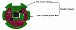
On a four-layer board, for example, one internal layer may be used for ground and another for power distribution. Depending on the design, the power layer may contain separate copper regions for rails such as 5 V, 3.3 V, and 1.8 V.
Split planes can save layers, but each region needs enough copper to provide a suitable path to its loads. Narrow necks and long, irregular routes should be examined carefully.
The stack-up should be selected according to the actual electrical requirements, current levels, routing constraints, and number of supply rails—not simply because a particular arrangement is common.
5. A Practical Checklist Before Manufacturing
Before releasing a PCB for fabrication, I would review the power distribution with these questions in mind:
I have also been exploring these practical considerations from the PCB fabrication perspective at PCBCool, particularly how copper geometry and board construction affect the manufacturability of a power-distribution design.
A regulator may be capable of supplying the required current, but a narrow copper path between the regulator and the load can introduce voltage drop and localized heating. This can become particularly important in low-voltage circuits, where even a relatively small drop may affect the operation of downstream electronics.
One way to improve power distribution is to use a PCB power plane or a suitably designed copper pour. However, simply increasing the copper area does not guarantee a good result. The actual current path, copper thickness, and layout restrictions all matter.
1. Why Does PCB Copper Geometry Matter?
The resistance of a copper path depends on its length, width, thickness, and material properties. For a simplified uniform conductor:
R = ρL / (WT)
Where:
- R is resistance.
- ρ is the resistivity of copper.
- L is the conductor length.
- W is its width.
- T is its thickness.
This matters in power supply designs because voltage drop is related to current and resistance:
V = IR
For example, a voltage drop that is insignificant on a higher-voltage rail may be more problematic on a low-voltage supply. A 100 mV drop on a 24 V rail represents a much smaller percentage of the supply voltage than the same drop on a 1.2 V rail.
A power plane can provide a wider distribution path, particularly when one supply rail feeds multiple loads across the board.
2. A Large Power Plane Can Still Have a Bottleneck
One layout issue worth checking is the narrowest section of the copper path.
A power plane may occupy a large area, but mounting holes, vias, component clearances, signal routing, and other copper regions can restrict the available path. If the current must pass through a narrow neck before reaching a load, that section may behave more like a narrow power trace than a broad plane.
When reviewing a layout, I would check:
- Where current enters the board and where it leaves the plane.
- Whether high-current loads have a reasonably direct path to the source or regulator.
- Whether vias, cutouts, or clearances create narrow sections.
- Whether several loads depend on the same restricted copper path.
- Whether the copper geometry remains adequate after routing is complete.
3. Copper Thickness and Thermal Performance
Copper thickness is another consideration in power distribution. For the same conductor geometry, 2 oz copper is approximately twice as thick as 1 oz copper, giving it lower resistance.
However, thicker copper is not always the only solution. Improving the width and continuity of the current path may also help, depending on the design requirements.
Resistive heating follows the relationship:
P = I²R
This means that reducing resistance can reduce the heat generated by current flowing through the copper. A wider copper area can also help distribute heat over a larger region.
For power MOSFETs, regulators, motor drivers, and other components that dissipate significant power, copper areas and thermal vias may help move heat away from the component. Their effectiveness still depends on the component, PCB construction, and overall thermal design.
Thermal reliefs also deserve attention. They make soldering easier by limiting heat flow into large copper areas, but they add resistance compared with a solid copper connection. For high-current connections, the electrical and thermal requirements should be considered alongside the assembly process.
4. Should Every Supply Rail Use a Power Plane?
Not necessarily. A properly sized power trace can be adequate for short connections, low-current rails, and relatively simple boards.
A power plane or copper pour becomes more useful when a rail must supply multiple loads distributed across the PCB, carry substantial current, or reach components without consuming too much routing space.
On a four-layer board, for example, one internal layer may be used for ground and another for power distribution. Depending on the design, the power layer may contain separate copper regions for rails such as 5 V, 3.3 V, and 1.8 V.
Split planes can save layers, but each region needs enough copper to provide a suitable path to its loads. Narrow necks and long, irregular routes should be examined carefully.
The stack-up should be selected according to the actual electrical requirements, current levels, routing constraints, and number of supply rails—not simply because a particular arrangement is common.
5. A Practical Checklist Before Manufacturing
Before releasing a PCB for fabrication, I would review the power distribution with these questions in mind:
- Is the copper path wide enough for the expected current?
- Has voltage drop been considered for sensitive low-voltage rails?
- Are there narrow sections between the power source and high-current loads?
- Is the selected copper thickness appropriate for the design?
- Are separate voltage regions properly isolated?
- Could the plane's shape or routing restrictions create a current bottleneck?
- Have thermal requirements around power components been considered?
- Have the copper regions been checked again after completing signal routing?
I have also been exploring these practical considerations from the PCB fabrication perspective at PCBCool, particularly how copper geometry and board construction affect the manufacturability of a power-distribution design.