Facebook
 Google
 GitHub
 Linkedin
Digital Electronics Basics: Understanding Logic Circuits
Learn about the logic circuits utilized in digital electronics with Boolean Algebra and Truth Tables.
Elementary circuits are the foundation of digital electronics applications. The proper grouping of these basic circuits makes it possible to create highly complex logic circuits. Even in a large-scale digital system, there are only a few basic operations to perform – these operations may be repeated many times. The logic gates usually used to carry out Boolean algebraic equations are the OR, AND, and NOT circuits.
Boolean Algebra
The English logician and mathematician George Boole introduced in 1854 an algebraic framework for a system comprising two states: true and false. This framework fundamentally started the area of computer science even before the presence of the integrated circuits currently utilized in digital logic.
The American mathematician Claude Shannon in 1930 applied Boole’s algebraic framework to his work on switching circuits, beginning the field of information theory and digital circuit design.
Modern digital circuit design widely uses the initial Boole framework, taking the name of Boolean algebra. But this term incorporates the work of the many contributors to the field after him.
Boolean algebra is helpful to analyze and simplify digital logic circuits. It allows computers to perform from simple to very complex operations.
A set of symbols and a set of rules to manipulate these symbols compose the Boolean algebra.
Some characteristics are:
- A logic expression, or logic function, is an equation showing each output in the circuit as a function of the inputs. If a circuit contains multiple outputs, then each output requires a logic expression.
- A set of symbolic operators define the logic operations.
- A logic function used to describe a single output can take on only the values 1 and 0.
- Variables are the different symbols in a Boolean expression. In the expression A + B = Y, A, B, and Y are the variables.
- The letter symbols can adopt either of two values, 0 and 1. In Logics, 1 signifies true, and 0 means false.
- The values assigned to a variable have a logical significance.
- Boolean algebra has three basic operations: OR, AND, and NOT.
- The dot symbol ‘∙’ (also ᴧ) means an AND operation, and the plus symbol ‘+’ (also ∨) means an OR process. For instance, A ∙ B means A AND B, and A + B means A OR B.
- It is also valid to omit the dot sign to indicate the logical connection by placing the letters next to each other as in AB = Y.
- Boolean algebra expresses the fundamental properties of logic operations, such as OR, AND, and NOT, and the set theory operations such as union, intersection, and complement. For example, the logical claim that both a statement and its negation cannot be true has an equivalent in set theory: the intersection of a subset and its complement is an empty set.
What is a Truth Table?
A truth table of a logic system lists all possible combinations of input binary variables and their resultant outputs. The logic system output comes from a logic expression – the Boolean expression – relating the system’s output and inputs.
A logic circuit’s truth table with n binary inputs will have 2ⁿ input combinations or rows. For example, with one input, there are only two possible values, 0 and 1; with two inputs, there are four input combinations: 00, 01, 10, and 11; with three inputs, there are eight input combinations: 000, 001, 010, 011, 100, 101, 110, and 111.
In all further discussion throughout this article, we will use the letters A, B, …, N to designate the n inputs to a logic system and the letter Y for the outputs.
Table 1 shows the truth table of the two-input logic system of figure 1. For this particular system, the output Y = 0 when A = B = 0, and Y = 1 for all other input combinations.
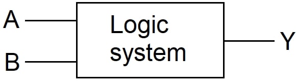
Figure 1. Two-input logic system.
| A | B | Y |
| 0 | 0 | 0 |
| 0 | 1 | 1 |
| 1 | 0 | 1 |
| 1 | 1 | 1 |
Table 1. The truth table for a two-input logic system.
Table 2 shows the truth table of the three-input logic system in figure 2. In this case, we assume that output Y = 1 when A = B = C = 1, and Y = 0 for all other input combinations.
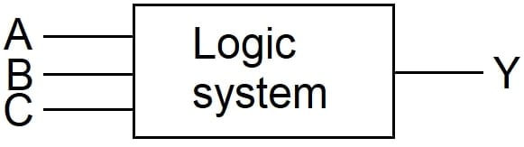
Figure 2. Three-input logic system.
| A | B | C | Y |
| 0 | 0 | 0 | 0 |
| 0 | 0 | 1 | 0 |
| 0 | 1 | 0 | 0 |
| 0 | 1 | 1 | 0 |
| 1 | 0 | 0 | 0 |
| 1 | 0 | 1 | 0 |
| 1 | 1 | 0 | 0 |
| 1 | 1 | 1 | 1 |
Table 2. The truth table for a three-input logic system.
What are Logic Gates?
Logic gates are the initial building blocks of digital systems. Each primary logic gate is a piece of hardware or electronic circuit employed to execute basic logic expressions.
The laws of Boolean algebra help manipulate binary variables and simplify logic expressions, but these are executed in digital systems through electronic circuits named logic gates. The three elementary logic gates are OR, AND, and NOT.
In the following discussion about logic gates, we disregard how voltages represent the 1’s and 0’s and their handling by transistors. This way allows us to go into the basics without describing the physical hardware.
The OR Gate
An OR gate has the following definition (positive logic): “the output of an OR gate acquires the 1 state if one or more inputs attain the 1 state.” The OR gate may have two or more inputs and one output.
The simple circuit diagram of figure 3 shows the basis of an OR gate.
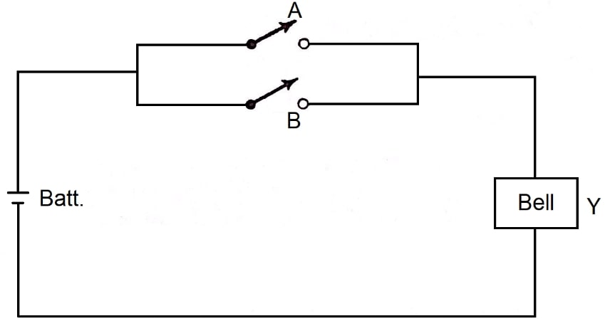
Figure 3. Principle of operation of an OR gate.
This circuit activates the bell Y from either of two switches, A or B. We can observe that A or B or both will ring the bell. Therefore, this is an OR circuit or an OR gate in switching logic terminology since A OR B = Y.
Although we employ three symbols in this example, we must remember that there are only two states: on and off. Assuming on = 1 and off = 0 (positive logic), we can say that 1 OR 1 = 1, meaning that if either or both switches are in the on (1) state, the bell will also be in the on (1) state.
As seen previously, in Boolean algebra, the “+” sign is a logical connection to indicate the OR function. Thus, A + B shows the expression A OR B, but not the arithmetic sum.
Figure 4 shows the standard symbol for the OR gate together with the Boolean expression for this gate. The expression states that Y equals A or B or … or N.
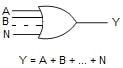
Figure 4. The standard symbol for an OR gate and its Boolean expression.
Note that Table 1 above matches the truth table for a two-input OR gate.
Some Boolean identities for the OR “+” gate are:
A + B + C = (A + B) + C = A + (B + C)
A + B = B + A
A + A = A
A + 1 = 1
A + 0 = A
The AND Gate
An AND gate has the following definition (positive logic): “the output of an AND gate acquires the 1 state if and only if all the inputs attain the 1 state.” The AND gate may have two or more inputs and one output.
The simple diagram of figure 5 shows the basis of an AND gate.
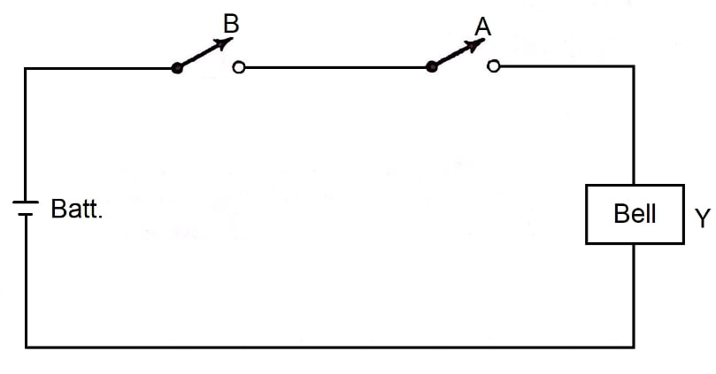
Figure 5. Principle of operation of an AND gate.
In this case, both switches A and B must be closed to ring the bell. Logically it can be established that A AND B = Y. In switching logic terminology, this configuration is an AND circuit or AND gate.
Note that 1 AND 1 = 1 – if both switches are in the on (1) state, the bell will also be in the on (1) state.
As seen before, in Boolean algebra, the dot “∙” sign is a logical connection to indicate the AND function. Thus, A ∙ B shows the expression A AND B, but not it's arithmetic meaning of multiplication. Skipping the dot sign is acceptable.
Figure 6 shows the standard symbol for the AND gate together with the Boolean expression for this gate. The expression states that Y equals A and B and … and N.
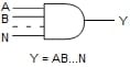
Figure 6. The standard symbol for an AND gate and its Boolean expression.
Note that Table 2, above matches the truth table for a three-input AND gate.
Some Boolean identities for the AND “∙” gate are:
ABC = (AB) C = A (BC)
AB = BA
AA = A
A1 = A
A0 = 0
A (B + C) = AB + AC
A + AB = A
A + BC = (A + B) (A + C)
The NOT or Inverter Circuit
A NOT circuit has one-input and one-output; its output is the complement of the input.
The logic negation has the following definition: “the output of a NOT gate is always in the opposite state of the input”.
If we designate an input signal as A, the output signal is NOT A. A line over its symbol indicates the complement or negation of a variable. Thus, Ā means NOT A, and if A represents 1, the expression Ā indicates 0. If A = 0, Ā = 1. In the same way \[\overline{1} = 0 \quad and \quad \overline{0}= 1. \]
Another common way to designate the NOT function is by placing a prime after the input variable, such as A’.
An additional name for this circuit is the inverter since it inverts the output with respect to the input.
The standard symbol for a logic negation is a small circle where a signal line joins a logic symbol. The inversion circle is a common way to show inversions in schematics.
Figure 7 shows a logic negation at the input, and figure 8 shows a logic negation at the output of a logic block.
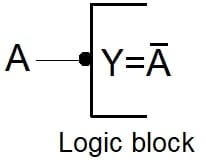
Figure 7. A logic negation at the input.
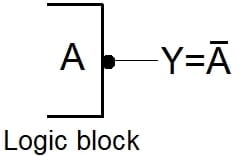
Figure 8. A logic negation at the output.
Figure 9 shows a familiar symbol for the NOT circuit together with the Boolean expression for this gate.
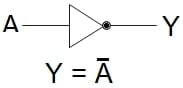
The expression states that Y equals NOT A, or Y is the complement of A.
Table 3 shows the truth table for a NOT or inverter logic gate.
| A | Y |
| 0 | 1 |
| 1 | 0 |
Table 3. The truth table for a NOT logic gate.
Some Boolean identities for the NOT gate are:
\[\overline{\overline{A}} = A\]
\[Ā + A = 1\]
\[ĀA = 0\]
\[A + ĀB = A + B\]
Understanding Logic Circuits
Boolean algebra is one of the primary tools that allow the logic designer to simplify complex logic expressions. This algebra comprises a set of symbols and the rules to manipulate them.
A truth table defines the functionality of a logic circuit. It lists every possible input combination to a logic circuit and its corresponding output.
The term logic gate designates a digital circuit that executes the most basic functions viable with the binary system.
The output of an OR gate will be 1 when any of the inputs is 1. The logic operator symbol is the plus sign “+.”
The output of an AND gate will be 1 only if all the inputs are 1. The logic operator symbol is the dot “∙.”
The output of a NOT gate is the complement of the input. The NOT operation is also called inversion. The symbol for the inverter is a small circle where a signal line joins a logic symbol.
Related Content