Facebook
 Google
 GitHub
 Linkedin
Biricha Lecture Notes on Analog and Digital Power Supply Design Part 2D
This article discusses the reasons why Proportional Integral Derivative (PID) controller is not best suited for stabilising most switch-mode power supplies.
Whether or not a Proportional + Integral + Derivative (PID) controller is suitable for stabilising power supplies has become an emotive debate rather than a scientific discussion. The debate has been compounded by the arrival of many digital power solutions, which seem to come as standard with a PID controller programmed in their software.
People like PID controllers for their simplicity and are reluctant to change what they know and love for something else that performs better, but needs a more delayed understanding of control theory. In this article we would like to present our reasons as to why, here at Biricha we try to avoid using PID controllers for the majority of the power supplies that we design. This is merely our opinion and is not intended to re-start a debate, and as such, we ask you to decide for yourselves as to whether or not PID is suitable for your application.
Introduction
PID controllers are extremely easy to design and implement. With less than 10 minutes on any search engine, you will find many analog and digital realizations; there are even automatic tuning algorithms. Whilst this controller and its close relative (PI) are excellent for stabilizing motor control systems or temperature controllers and the like, it is our opinion that they are unsuitable for compensating most switch-mode power supplies. Furthermore, although one may be able to get away with using a PID controller in a current mode converter or a PSU with lots of ceramic caps on the output there are better alternatives. If you do intend to use a PID controller, we highly recommend reading the excellent analysis by Christophe Basso which was presented at APEC in 2011 and is available for free on Mr Basso’s website [1].
The main attraction of PID is that one does not need to know much about control theory, frequency response analysis, pole-zero placement, phase margin, gain margin, stability criteria, etc etc. Instead, you heuristically (i.e. scientific word for semi-educated trial and error ) change the compensator’s 3 gain terms to achieve the desired response. Though this method is extremely effective in millions of applications, we feel that it is not suitable for power supply design. Most experts agree that switching power supplies should be designed in the frequency domain, and yet PID is a tool whose main advantage is that you don’t design in the frequency domain! This is a contradiction and, therefore, you can see from the onset that PID is not suitable for what we are trying to do, even though it is ideal for many other applications.
PID Compensator Explained
The transfer function of the PID is shown in the following equation:
Where, Kp is the proportional gain, Ki is the integral gain, Kd is the differential gain and s is the Laplace operator.
The design procedure is usually based around simply changing these gains until our control system’s transient response becomes satisfactory after a unit step. Please note that we are now working in the time domain and not frequency domain. However, almost everyone agrees that we should design our power supplies in frequency domain to ascertain a measure of our relative stability. So, how does changing these gains heuristically impact our poles and zeros in the frequency domain? How do we assess that we do not violate the stability criteria? Let us find out!
If we take common denominators on the previous equation, we will have:
You can immediately see that the numerator is a simple quadratic equation i.e. we have 2 zeros and in the denominator we have only 1 pole, which is at the origin. Please note that for a realizable system we need another pole, but this will have to be placed so high in frequency that it does not impact the transfer function at the frequencies of interest (or it would not be a pure PID )
To find the zeros, we need to solve the quadratic using:
In our case a = Kd, b = Kp and c = Ki; substituting these in the above equation we have:
Looking at the equation above you will see that the positions of both zeros and the pole at origin are inter-dependant on all three gains. This means that if you change any of the gains you will mess up the position of everything in frequency domain!
If you wish to place your pole and zeros intelligently, then you will have to derive the modulus and the phase of the transfer function, then solve several equations simultaneously and place the 2 zeros and the only pole in such a way so as to meet the stability criteria (please see our previous articles about loop stability).
Hang on, I hear you say; wasn’t the whole point of PID that we did not have to do this sort of analysis? The answer is yes, but we have to do this to show why it will not work very well! If you are already convinced, then please stop reading the rest of this article and pick up one of the many fantastic books in this field, written by experts and design a proper Type III compensator. There are several excellent books on the market (e.g. Basso, Erickson & Maksimovic), but for an eloquently written section on loop stability, and simple explanation of control loops, I really like Mr Maniktala’s Red A to Z book [2].
So Why Will Our PID Not Work Very Well?
Voltage Mode PSU performance with a Type III compensator
From figure 1 you can see an optimally compensated voltage mode power supply with a Type III compensator using our WDS software [3]. You can see that we have got good cross-over, phase margin and gain margin. We have also marked danger zones you should try and avoid crossing at.

Figure 1: Optimally compensated voltage mode power supply with a Type III compensator using our WDS software
For this power supply, we have kept the default values so that you can use our evaluation version to reproduce these experiments exactly. Please just download a free copy from our website (www. biricha.com/wds) and you can repeat these experiments yourselves.
WDS also allows you to run a spice simulation using LTSpice and figure 2 is the result of a 50% step load. You can see that our Type III compensator is performing very well.
Voltage Mode PSU performance with a PID compensator
Now let us see if we can design a PID compensator in WDS with a similar performance. In order to do this, all you have to do is to select a Type III and then manually set the two poles (not the pole at the origin) to 10MHz so that they do not impact the control loop. You now have a PID controller.
With a PID, we only have 2 zeros and one pole at origin. In order to meet the stability criteria, we must place our zeros at around the resonance frequency, otherwise we will cross with a sharp slope. We can then use the pole at origin to get a high gain at low frequencies and good cross over. (Please see our previous articles on this subject).
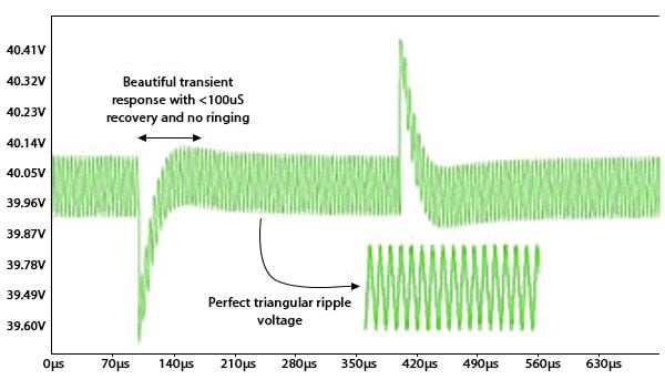
Figure 2: Type III compensator is performing very well
So if we cancel the 2 plant poles with our 2 PID zeros and then place our PID’s pole at the origin, the gain of our open-loop frequency response will be rolling off at a rate of 20 dB/decade.
We will then hit our capacitor’s ESR zero. If our gain is going down at 20dB/decade and then hits a zero, then the gain plot will go flat with a gradient of 0dB/decade. There are only 2 alternatives: either it will go flat before we cross over, i.e. we don’t cross at all, or it will go flat after we cross over i.e. we may end up with very little gain margin.
The best way to get a good feel of this is to simulate. You can simply download the evaluation version of WDS and keep all the default values. In the “Controller Design” tab under “Controller Poles and Zeros” select “Manual Placement” then set the two zeros at the resonant frequency (~1.7kHz), set “First Pole” and “Second Pole” to 10MHz to minimize their impact and then experiment with the “Pole at the Origin”, you will see how hard it is to cross at a reasonable position without violating the stability criteria. You can then run an LT Spice simulation from within WDS from the Spice Simulation Tab.
Let us first see what happens if the loop does not cross:
Figure 3 shows the loop response with our PID’s pole and zeros placed in such a way that the loop goes flat before we cross the 0dB axis. Please note that Bode’s stability terms such as gain margin and phase margin are only defined at crossover frequency. If we do not cross, then we have absolutely no idea of whether this power supply is stable or not. We can either resort to looking at the Nyquist plot (even more analysis) or make sure that we do cross.
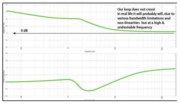
Figure 3: Spice simulation of the PSU’s output ripple voltage
Now let us look at Spice simulation of figure 3 PSU’s output ripple voltage:

Figure 4: How are we going to make this power supply stable
The figure 4 does not even take into consideration that we don’t have Kp, Ki and Kd’s relationships with the positions of our pole and zeros and that they are inter-dependant! How are we going to make this power supply stable “heuristically” by playing with these values?
The short answer is that we can’t without a great deal of mathematical analysis in frequency domain! Fortunately, WDS will do this for you, but we have lost the main advantage of PID’s which was its ease of design in the time domain.
Now what if we do cross? Can we get a better performance? The answer is no. In the following figure, we changed the position of the pole at the origin in WDS to make sure that the loop does cross at 20kHz just like our Type III. But please have a look to figure 5 at our gain; from our crossover up to half the switching frequency (Fs), we are only 2dBs below the 0dB point! This may work in this simulation, but in real life, the loop may cross the 0dB point many times! This is very dangerous; it is certainly not a product you can ship! Again, we recommend having a play with WDS yourself to see if you can get a good response.

Figure 5: We are only 2dBs below the 0dB point
Current Mode PSU with PID Controllers
It is certainly possible to stabilize a current mode PSU with a PID controller. After all, at low frequencies, our plant’s transfer function “looks” like a first-order system and we usually use a Type II compensator which ONLY has one zero, one pole at origin and extra pole.
So our PID only has one pole less than a Type II. The Type II’s extra pole is usually used to cancel the capacitor’s ESR zero; so with this pole missing again our loop will go flat at some point. However, if we derived the mathematical relationships between Kp, Ki, Kd and our pole and zeros then by clever pole-zero placement, we could possibly get a relatively stable power supply. The question is, if we need to do all these derivations, why not just use a Type II?
PID and Digital Controllers
The use of PID has been suggested by almost all digital power supply IC vendors. The irony, of course, is that digital power supplies are by far more susceptible to instability when used with a PID than analog ones [4].
The reason is that the phase in a digital power supply deteriorates much faster than an analog equivalent. This extra phase erosion is due to the sampling and reconstruction on our discrete time system. The net result is that our phase usually crosses the -180 degree point and therefore we must have at least 10 dB of gain margin. However, with the loop flattening, the gain margin will be poor.
In figure 6 we have used WDS to design a digital power supply with similar specification to the analog ones (please note that the change in the specification was necessary to make sure that the spice completed the simulation in a reasonable time).

Figure 6: We have used WDS to design a digital power supply with similar specification
You can easily see how much faster the phase is rolling off compared to an analog supply. Furthermore, as it crosses the -180 degree point our gain margin is very poor indeed. The spice simulation of the step response for this power supply is shown in figure 7.
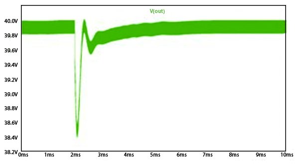
Figure 7: The spice simulation of the step response
Note that even though we have 70 degrees of phase margin, due to the low gain margin, we still have large undershoot and ringing. We must stress at this juncture that, this is only a simulation and a digital power supply in real life, with this specification, will almost certainly be completely unstable for many different reasons.
Concluding Remarks
In this article, we discussed why we feel that a PID controller is not best suited for stabilising most switch-mode power supplies. We supported our hypothesis with transfer function analysis and various simulations in both frequency and time domain. We believe that switch mode power supplies are best designed in the frequency domain and presented the main downfall of PID as the need to heuristically adjust the gain terms in the time domain.
PID controllers are excellent for thousands of applications; millions are in use right now, but in our opinion, there are superior alternatives to PID for compensating switch-mode power supplies.
Things to Try
- Download a copy of Biricha WDS PSU Design software from www.biricha.com
- Attend one of our Analog or Digital Power Supply Design workshops
About the Author
Dr. Ali Shirsavar works as the Director at Biricha Digital Power responsible for the design and presentation of industrial workshops on the field of power electronics, power supply design and digital power. He is specially skilled in the field of power electronics, power supplies and embedded systems. He earned his Bachelor's Degree in Electronics Engineering and his Doctor of Philosophy in Power Electronics both at the University of Reading at located in England.
Bibliography
- “The Dark Side of Loop Control Theory” by C. Basso, APEC 21011 http://cbasso.pagesperso-orange.fr/Downloads/PPTs/Chris%20 Basso%20APEC%20seminar%202012.pdf
- “Switching Power Supplies A - Z, Second Edition 2nd Edition” by Sanjay Maniktala ISBN-13: 978-0123865335
- Biricha Digital’s “Analog PSU Design Workshop” Handbook
- Biricha Digital’s “Digital PSU Design Workshop” Handbook
Related Content