Facebook
 Google
 GitHub
 Linkedin
A SiC MOSFET for Mainstream Adoption
This article highlights Infineon CoolSiC™ semiconductor solutions with an implementation of a 1200 V CoolSiC™ MOSFET in three-phase Si based solutions.
To become a mainstream product, the silicon carbide (SiC) MOSFET ́s outstanding technical functionality must come together with the right cost position, system compatibility features, silicon-like FIT rates and volume manufacturing capability. These multiple levers must all match within a working business case for power system manufacturers in order to change the game in power conversion. This especially targets energy efficiency and making “more out of less”.
Infineon shows the corresponding feature set of the CoolSiC™ MOSFET family and matching driver ICs. These support entry applications like photovoltaic inverters, uninterruptible power supplies (UPS), drives, battery charging infrastructure and energy storage solutions.
A growing number of power electronics applications can no longer address the future target requirements when relying on silicon (Si) devices alone. Improving power conversion performance while increasing power density, reducing board space and driving down component count as well as system cost are conflicting challenges due to silicon devices’ high dynamic losses. To fix this, engineers are increasingly deploying solutions with power semiconductors based on silicon carbide (SiC) material.
Infineon and SiC Schottky diodes have been an innovative duo for a long time now, with first 600V products launched in 2001. Over the years a broader portfolio including 650V and 1200V voltage classes has grown. New generations with higher current handling capability per given chip area while reducing power losses were developed and released. Hundreds of millions of SiC diode chips have been produced and shipped to the market. In applications such as MPP tracking in solar inverters or power factor correction in switch-mode power supplies, the use of a Si IGBT plus SiC diode or a super-junction Si MOSFET with SiC diode became a state-of-the-art solution for more than a decade now, achieving high conversion efficiency and highly reliable systems.
SiC Technology
Market reports even highlight that a plateau of productivity is being entered for SiC diodes [1]. Volume manufacturing skills in SiC technology, production quality monitoring and a field track record with excellent FIT rates built a base for taking the next step in product strategy encompassing also a SiC MOSFET. Transistor functionality in SiC semiconductor material provides further potential for getting out more of less energy - energy efficiency – in the whole electrical energy supply chain from energy generation, transmission and distribution to consumption.
Boosting Efficiency Factors
Let ́s take a closer look at the performance advantage of a SiC MOSFET versus a Si IGBT. Figure 1 shows an example of a state-of-the-art silicon solution: one phase-leg of a three-level T-type topology with 650V and 1200V silicon (Si) IGBTs typically used in three-phase systems like photovoltaic inverters and UPS if high efficiency and high power density are targeted. High efficiency can be reached up to a switching frequency of 20kHz to 25kHz [2] with such a solution.

Figure 1: Comparison of efficiency for a 1200V SiC MOSFET (45mOhm typ., IMW120R045M1) versus 1200V Si IGBT (40A, IKW120N120H3) in outer switch positions, in a three-level (3L) T-type topology, one phase-leg. For the 72 kHz operation case, 650V SiC diodes are replacing Si diodes in the inner switch positions.
A 1200V SiC MOSFET converts current at about 80% lower losses than a 1200V Si IGBT thanks to low device capacitances, low partial load conduction losses and the absence of a current turn-OFF tail. Using 1200V SiC MOSFETs in the outer switch positions boosts efficiency significantly and enables higher output power for given frame size. Raising switching frequency further would quickly deteriorate efficiency and maximum output power for the Si-based solution, while a SiC MOSFET ́s low switching losses make this possible.
Demonstrated by this example, a tripling of the operating frequency up to 72kHz still results in higher efficiency than achieved by the silicon solution operated at 24kHz. As a result, reduction of the physical size of passive components, lower cooling effort, reduced system weight, and cost can be achieved.
Another three-phase power conversion example is charging infrastructure for electric vehicles. A 1200V SiC MOSFET enables building one LLC full-bridge stage for the DC-DC conversion stage, where a typical silicon solution relies on 650V Si super junction MOSFETs where then two cascaded LLC full-bridges are needed to support the DC link of 800V.
Comparison of 1200V SiC MOSFET and 1200V Si IGBT
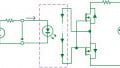
As shown in Figure 2, four sets SiC MOSFET plus driver ICs can replace eight sets of Si super junction MOSFETs plus driver ICs. Other than the reduced part count and board space, also efficiency may be optimized. For a SiC MOSFETs solution, only two switch positions are turned on in every ON-state, in comparison to four switch positions in the Si solution. Highly efficient charging cycles can be realized by using a SiC MOSFET in fast battery charging.

Figure 2: Three-phase LLC DC/DC stage comparison for same power rating, showing reduced part count and benefit in ON-state current path if 1200V SiC MOSFETs (right) rather than 650V super-junction Si MOSFETs (left) are used.
Thanks to dynamic losses being an order of magnitude lower than in the 1200 V Si-class, a SiC MOSFET also gives traditional simple topologies a revival by increasing performance. In Figure 3, a conventional two-level solution using 1200V SiC MOSFETs is compared to the previously mentioned state-of-the art three-level silicon solution. Benefits by a two-level topology are far simpler control schemes and reduced the part count by 50%. Such a solution can be used in photovoltaic and UPS inverters, as well as inactive front-ends with bidirectionality in drives systems, battery charging and energy storage.

Figure 3: Comparison of efficiency for a 1200V SiC MOSFET (45mOhm typ., IMW120R045M1) in a two-level (2L) configuration versus a three-level (3L) T-type configuration using 1200V and 650V Si IGBTs, one phase-leg. Efficiency increase from PCB layout improvement and inductor core losses improvement are shown respectively
solutions. As can be seen from Figure 3, despite doubling the switching frequency from 24kHz to 48kHz a 0.3% to 0.4 % efficiency increase results at high load condition for a two-level SiC MOSFET solution, which indeed is impressive as the switching voltage is doubled compared to three-level operation – 800V versus 400V.
However, there are also challenges when designing in a SiC MOSFET. The switching transients of a SiC MOSFET must be considered. A dv/dt of 50 V/ns or more is not unusual in comparison to 5 to 20V/ns typically seen in a 1200 V Si IGBT. A parasitic coupling capacitance on board level will thus lead to excessive energy loss. For the case of replacing a three-level Si IGBT solution with a simpler two-level solution, the parasitic coupling capacitance will generate eight times higher energy losses if switching voltage and frequency both are doubled.
Figure 3 shows the original efficiency line when a SiC MOSFET is used plug and play in a standard IGBT two-level solution, while the next efficiency line shows how a careful PCB design with respect to drain-source parasitic board capacitance will contribute to reducing the losses [2]. A second topic to consider when switching frequency is increased concerns the core losses of the inductor. With ripple current and its corresponding loss staying constant over the whole load regime, an improvement of core losses by changing the core material influences mainly the partial-load efficiency.
These two improvements finally resulted in the attractive efficiency line above 98.5 % versus the three-level Si IGBT solution. This demonstrates that a SiC MOSFET is mostly not a plug and play option to Si IGBT and significant design-in work is required to bring performance to a higher level. One of the development targets for Infineon ́s CoolSiC™ MOSFET, therefore, was to tune device parameters to values making system design implementation as easy as possible.
System Compatibility
One system compatibility feature is the gate driving scheme. Until now, SiC MOSFETs required a higher gate drive voltage than Si IGBTs or Si MOSFETs and usually suffer from a low gate-source threshold voltage with just minor margin to zero volts. This minor margin makes gate voltage ringing spikes at high dv/dt slew rates a concern for the system designer.
The novel trench technology introduced with Infineon’s CoolSiC™ MOSFET enables a standardized gate driving scheme as for Si IGBTs with +15 V being sufficient for turn-ON, and a benchmark threshold voltage of 4 V for a robust signal to noise ratio during current turn-OFF. SiC MOSFETs also require matching driver ICs to unlock their full potential. These drivers must handle high dv/dt reaching 50 V/ns or above, and high switching frequencies, posing tougher requirements on timing and tolerances.
A SiC MOSFET might also need negative gate voltage, especially when used in hard-switching topologies, or a Miller clamp. Infineon ́s EiceDRIVER™ ICs are well-suited to drive SiC MOSFETs, and come in a broad portfolio offering various features depending on application needs [3]: tight propagation delay matching, precise input filters, wide output-side supply range, negative gate voltage capability or Miller clamping, and extended CMTI capability.Reliability and robustness assuranceReliability and robustness assurance in SiC are strongly linked to Si mainstream technologies. With Infineon ́s long track record in power semiconductors and understanding of application needs, tough requirements were set for CoolSiC™ MOSFET products. SiC is a great power semiconductor, however designing a MOSFET in this material involves technological challenges for tuning of performance parameters versus reliability and robustness.
Designing a planar SiC MOSFET
Designing a planar SiC MOSFET is a major trade-off between area-specific ON-resistance and gate oxide reliability, in other words, “chip cost and performance versus reliability”. The defect density on the planar SiC – SiO2 interface is very high in 4H-SiC [4], which leads to scattering of electrons in the MOSFET channel and thereby a reduction of electron channel mobility. The reduced performance shows up as increased channel resistance and increased power losses in ON-state. Only by applying an excessive electric field across the oxide for turn-ON, either via higher gate-source voltage or thinner SiO2 layers the area-specific ON-resistance can be kept on an attractively low level.
Trench MOSFET Device Structure in SiC Material
For a trench MOSFET device structure in SiC material, the need to overdrive the oxide is not in place thanks to SiO2 interface in the vertical crystal lattice plane having a far lower defect density than a planar interface [5]. However, a trench structure is a bigger challenge with regards to blocking mode at the trench corners due to high electric fields in SiC material. Design measures to achieve a proper field reduction are more complex than in planar structures. CoolSiC™ MOSFETs contain a unique asymmetric trench structure [6] reducing the electric field in OFF-state, see Figure 4.

Figure 4: Schematic cross-section of the CoolSiC™ MOSFET cell.
A large portion of the bottom of the trench is embedded into p+ wells, which extend below the bottom of the trench thus reducing the OFF-state electric field. For gate oxide reliability as described in [6, 7] the resulting extrapolated 20 years operation lifetime of the product at an ON-state operation of +15 V, shows a predicted low failure rate including extrinsic defects of 0.2ppm.
Gate threshold voltage stability has also been a concern for SiC MOSFETs for a long time. A well-optimized MOS process is required for guaranteeing a narrow and predictable drift [8] over a lifetime, a pre-condition for a datasheet specification of this parameter.
As can be seen in Figure 4, the large area of the p-emitter also enables the device to be used as a rapid free-wheeling diode. It is a strong value adder for a SiC MOSFET in many applications if the intrinsic diode can be utilized, as no extra SiC Schottky diode is needed. This intrinsic diode comes with high commutation robustness and low reverse recovery charge [7].
The CoolSiC MOSFET intrinsic diode is reliable in long term operation, Figure 5 demonstrates this by a performed DC current stress test: forward voltage (VF) and on-resistance (RDSon) correlations before and after stress have proven that the intrinsic diode is stable and ready to be used.

Figure 5: DC stress test result of an intrinsic diode of CoolSiC™ MOSFET. Test conditions: VGS=-9 V, 20 A per chip, Tvj~150°C. VF and RDSon correlations after >100h DC operation.
Infineon was pioneering in SiC MOSFET studies as can be seen from publications from the 90s [9]. The deep knowledge of the limits and options, the strong internal benchmark and the quality of Si-MOS technologies was the fundament for the decision on the CoolSiC™ trench technology. CoolSiC™ MOSFET products now come with robustness levels equivalent to Si IGBT based systems, as illustrated in Figure 6.
Volume Capability
Before the widespread adoption of SiC MOSFETs can take place, customers will need to be sure that their chosen supplier will be able to provide a consistent supply of high-quality products, and continues to deliver when demand increases. Established production flows at Infineon for high volume and high flexibility are proven for both Si and SiC chip manufacturing, as well as for assembly into discrete packages or power modules. Advanced power device technologies have successfully been ramped before, e.g. CoolMOS™, TRENCHSTOP™ IGBT, and CoolSiC™ Schottky diodes. The company ́s skills are in place to also bring CoolSiC™ MOSFET products through a market introduction and volume ramp.

Figure 6: Novel CoolSiC™ MOSFET technology from Infineon comes with robustness levels equivalent to IGBT based systems.
Cost Position
One of the factors that historically blocked broader adoption of SiC devices in the market was the higher price compared to silicon devices. Still, SiC devices are more expensive and cost parity will not be reached in a foreseeable future due to fundamental differences to silicon in the fabrication process of raw wafers.
SiC diode prices have declined over the years as a result of increased adoption, the economy of scale, new area-effective chip designs and moves to larger wafer diameters in production. The lower prices and increased availability of SiC devices in the market have now resulted in renewed demand from power designers who are under pressure to improving power conversion performance while reducing system cost at the same time. The first entry applications for CoolSiC™ MOSFET meanwhile are successfully ramping up where a total system cost reduction can be achieved with today ́s price level.
These first applications are triggering future volume growth for productivity improvements via economy of scale, and over time, there is an attractive cost-down roadmap for SiC in comparison to Si technologies as illustrated in Figure 7.

Figure 7:Exemplary view on productivity potential for SiC chips, and corresponding system costs.
Moving Toward an Energy Smart World
CoolSiC™ semiconductor solutions are the next step towards an energy-smart world. It is shown in this article how the implementation of a 1200 V CoolSiC™ MOSFET in state-of-the-art three-phase Si-based solutions can increase efficiency by more than 0.5%, reduce part count by 50%, as well as triple the switching frequency to 72kHz at an even higher efficiency than a Si IGBT solution operated at 24 kHz.
CoolSiC™ MOSFET together with EiceDRIVER™ ICs hereby offers a new degree of flexibility for system designers to improve on efficiency, save space and weight, reduce cooling requirements and improve reliability while achieving lower system cost. CoolSiC™ MOSFET family will match all the key requirements for a broad market adoption in various power conversion schemes including performance, cost position, system compatibility features, silicon-like FIT rates, and volume manufacturing capability.
About the Author
Fanny Björk began to study Electrical Engineering at KTH in Stockholm with a focus on electro-physics. She earned an Industrial Doctoral Service in collaboration with ABB with a focus on silicon carbide SiC, process optimization and component design. Currently, she holds a Master's Degree in Electrical Engineering and a PhD in Solid-State Electronics both earned at KTH Royal Institute of Technology. She works at Infineon Technologies as the Product Marketing Manager for Silicon Carbide.
References
- Yole Power SiC 2017 Materials Devices and Applications Yole Development
- Sobe, Brucchi. “Experimental study of Si- and SiC-based Voltage Source Inverters”. Proc. PCIM 2017 Nuremberg.
- Infineon industrial galvanic isolated gate driver ICs
- Das MK, Um BS, Cooper JA, “Anomalously high density of interface states near the conduction band in SiO2/4H-SiC MOS devices”, Materials Science Forum, Vol.338-3, 1069-1072, 2000
- Kimoto. T. et. al., “Interface Properties of Metal–Oxide–Semiconductor Structures on 4H-SiC{0001} and (1120) Formed by N2O Oxidation”,Japanese Journal of Applied Physics, Volume 44, Part 1, Number 3, 2005.
- D. Peters et.al: "The new CoolSiC™ Trench MOSFET Technology for Low Gate Oxide Stress and High Performance", May 2017, Proc. PCIM 2017, Nuremberg
- CoolSiC™ 1200 V SiCMOSFET
- Aichinger et al. "Threshold voltage peculiarities and bias temperature instabilities of SiC MOSFETs Microelectronics Reliability 80" (2018) 68–78
- D. Peters et. al., “An 1800 V triple implanted vertical 6H-SiC MOSFET”, IEEE Transactions on Electron Devices, Volume: 46, Issue: 3, 1999
This article originally appeared in the Bodo’s Power Systems magazine.