Facebook
 Google
 GitHub
 Linkedin
IMEC Reports New Method To Fabricate Ultra-Thin Silicon Solar Cells
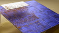
IMEC is developing a new method to produce ~50µm thin crystalline silicon wafers for use in solar cells. Theprocess involves mechanically initiating and propagating a crack parallelto the surface of a Si wafer. In this way, Si foils with an area of 25cm² and a thickness of 30-50µm have already been produced. The method makes use of industrially available tools (screen printer, belt furnace) and is potentially kerf-loss free.
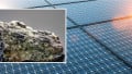
IMEC claims that adding an ultra-thin wafer or foil of active silicon on top of a low-cost substrate is a promising solution to reduce the amount of high-gradesilicon used in solar cells. IMEC is pursuing different paths to produce such foils of crystalline Si at an acceptable cost. One of the promising methods is a lift-off process that only requires the use of a screenprinter and a belt furnace; no ion-implanted or porous layer is needed. A metallic layer is screen printed on top of a thick crystalline Si wafer, which is then annealed in a belt furnace at a high temperature. When the wafer cools, the mismatch of the thermal expansion coefficient between the metal and the silicon induces a stress field in the substrate.
The stress field grows, initiating and propagating a crack in the silicon, close to and parallel with the surface. Next, the top layer of the silicon and the attached metal layer snap off from the parent substrate. The metal layer is removed from the silicon foil in a metal-etching solution, resulting in a clean and stress-free ultra-thin silicon foil. The substrate can be re-used to peel off further layers.
The process was demonstrated on both single- and multi-crystalline silicon, as well as on Cz (Czochralski or a method of crystal growth used to obtain single crystals of semiconductors) material with different orientations. IMEC already produced foils with an area of 25cm2 and a thickness of 30-50µm.
One of the resulting thin Cz foils was further processed into a solar cell using a heterojunction emitter process. The 1cm² cell reached an efficiency of 10.0%, without back-surface passivation or intentional surface texturing. These preliminary results indicate that the quality of the material is largely preserved during the lift-off process, in spite of the large stresses involved. IMEC expects to reach much higher efficiencies with added surface passivation and texturing.