Facebook
 Google
 GitHub
 Linkedin
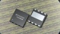
Imec Processes First Power Devices on 200mm CMOS-Compatible GaN-on-Si
Imec and its partners in the GaN industrial affiliation program (IIAP) have produced device-quality wafers with GaN/AlGaN layers on 200mm silicon wafers. With these wafers, functional GaN MISHEMTs were processed using standard CMOS tools. The used processes are compatible with the strict contamination rules in a standard CMOS processing line (e.g. no use of gold). These first GaN devices on 200mm wafers are an important milestone on the path to cost-effective production of power devices in high-productivity 200mm fabs.
GaN is a promising material for next-generation power devices with a performance beyond what is possible with silicon. Imec has recently succeeded in producing 200mm GaN-on-Si wafers with crack-free surfaces and a bow of less than 50µm. The wafers were made using an advanced MOCVD system from Applied Materials. The ability to use 200mm wafers is an important milestone, because it brings processing in reach of regular high-productivity 200mm fabs, allowing for an important cost reduction compared to processing smaller wafers on dedicated processing lines.
A second prerequisite for cost-effective processing, next to the wafer size, is that power devices can be fabricated with processes that are compatible with standard CMOS processes and tools. Imec proved this by processing its GaN-on-Si wafers using standard CMOS tools, yielding functional GaN MISHEMTs (metal-insulator-semiconductor HEMT). All equipment was verified for its capability to handle the wafers, and required only minimal adjustments in software and hardware. Conventionally, gold is used for ohmic contacts and gate structures in power devices, but it makes GaN processing incompatible with conventional CMOS processing. To overcome this, imec based the ohmic contact formation on an Au-free metallization system, and modified the Schottky gate to a gate dielectric based gold-free metal-insulator-semiconductor (MIS) structure. This introduction of the MISHEMT structure had the added advantage of reducing the high leakage current of conventional HEMTs.