Facebook
 Google
 GitHub
 Linkedin
Bizen Transistors: A Power Device Yielded From Quantum Mechanics
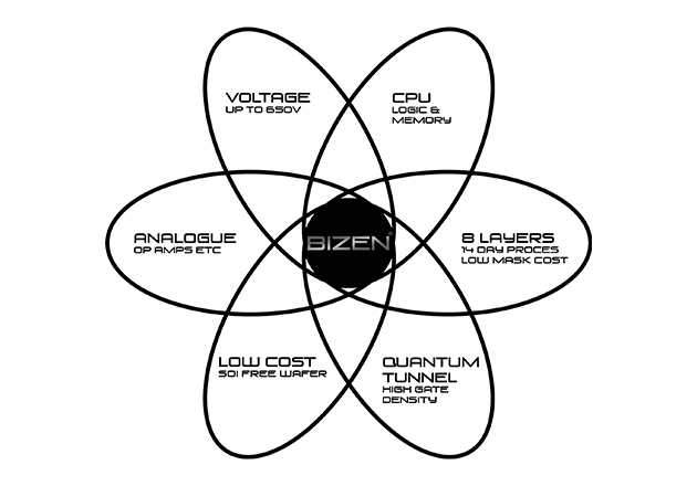
With claims of resetting Moore’s Law, Bizen Technology allows for a full range of digital, analog, and high voltage power devices to be developed through quantum mechanics within 14 days time to market rather than the industry-standard of 12 weeks.
The Nottingham-based, Search For The Next (SFN) is a fabless semiconductor group with a mission to find new ways to improve manufacturing time and costs for the development of advanced semiconductor processes and CPU architectures.
A patent-pending wafer process, that’s an alternative to MOS and bipolar technology. Image used courtesy of Wafer Train (SFN subsidiary).
Toward the end of 2018, SFN began a partnership with the UK’s Semefab, a fabrication facility that focuses on efficient power switching technologies in SiC and GaN, and through this collaboration invented the Bizen technology.

Bizen uses Zener quantum tunnel mechanics to provide a different way to isolate the base well called the ‘Tunnel’ terminal. Image used courtesy of Wafer Train (SFN subsidiary).
Allan James, CEO of Semefab, acknowledged the significance of the development of Bizen technology in retrospect to Moore's Law.
“If Bizen had been discovered back in the late ’60s when the transition from Bipolar to MOS and CMOS took place in order to cost-effectively integrate logic functions, it is possible that the industry may have developed strongly in the direction we are now proposing,” James said in a news release.
Bizen Technology Within Industry Known TO247 & TO263
The industry-standard TO247 and TO263 power MOSFET packages are some of the first devices that will utilize Bizen technology. For TO263, these N-channel Power MOSFETs exhibit low on-resistance and optimized switching characteristics, rendering them suitable for the most demanding high-efficiency converters. The TO247 are N-channel enhancement-mode power MOSFETs that will show extremely high packing density for low on-resistance, rugged avalanche characteristics, and low gate charge.
The CEO and Founder of SFN David Summerland discussed the versatility of Bizen technology with these industry-standard devices, “To get this level of performance from traditional silicon-based MOSFETs, the device size must be much bigger. A 1200V/75A in a TO247 housing can be achieved using wide bandgap materials like silicon carbide, but this approach has other well-known issues.”
Benefits of Bizen Technology
According to Bizen, these transistors can deliver the same voltage levels, switching speeds, and power handling performance of wide-bandgap devices. The first set of devices to use Bizen technology are Quantum Junction Transistors (QJT), which includes three parts rated at 1200V/75A, 900V/75A, and 650V/32A.
Standard bipolar or CMOS technology requires a gate resistor to be used to slow down the turn-on and turn-off of the MOSFET. By integrating Bizen technology, the device is able to eliminate the need for an external resistor which will allow designers to take advantage of the now-controllable current. Bizen technology allows for standard MOSFETS to become quantum tunneling transistors that provide lower dynamic power, higher switching speeds, and fewer process layers that results in less material used.
We can expect a simpler structure enabled by Bizen technology that will allow designers to create complex circuits with far fewer layers and increased logic density. In addition, these devices can be made using standard silicon substrates on conventional, larger-geometry silicon processing lines.